MX7828KCAI データシートの表示(PDF) - Maxim Integrated
部品番号
コンポーネント説明
一致するリスト
MX7828KCAI Datasheet PDF : 12 Pages
| |||

CMOS, High-Speed, 8-Bit ADCs
with Multiplexer
CS
tCSS
RD
ANALOG
CHANNEL
ADDRESS
RDY
tAS
ADDR
VALID
tAH
tRDY
tRD
tCRD
tINTH
tCSH
tCSS
tRD
tP
tAS
ADDR
VALID
tAH
tRDY
tCSH
tINTH
INT
tACCI
DATA
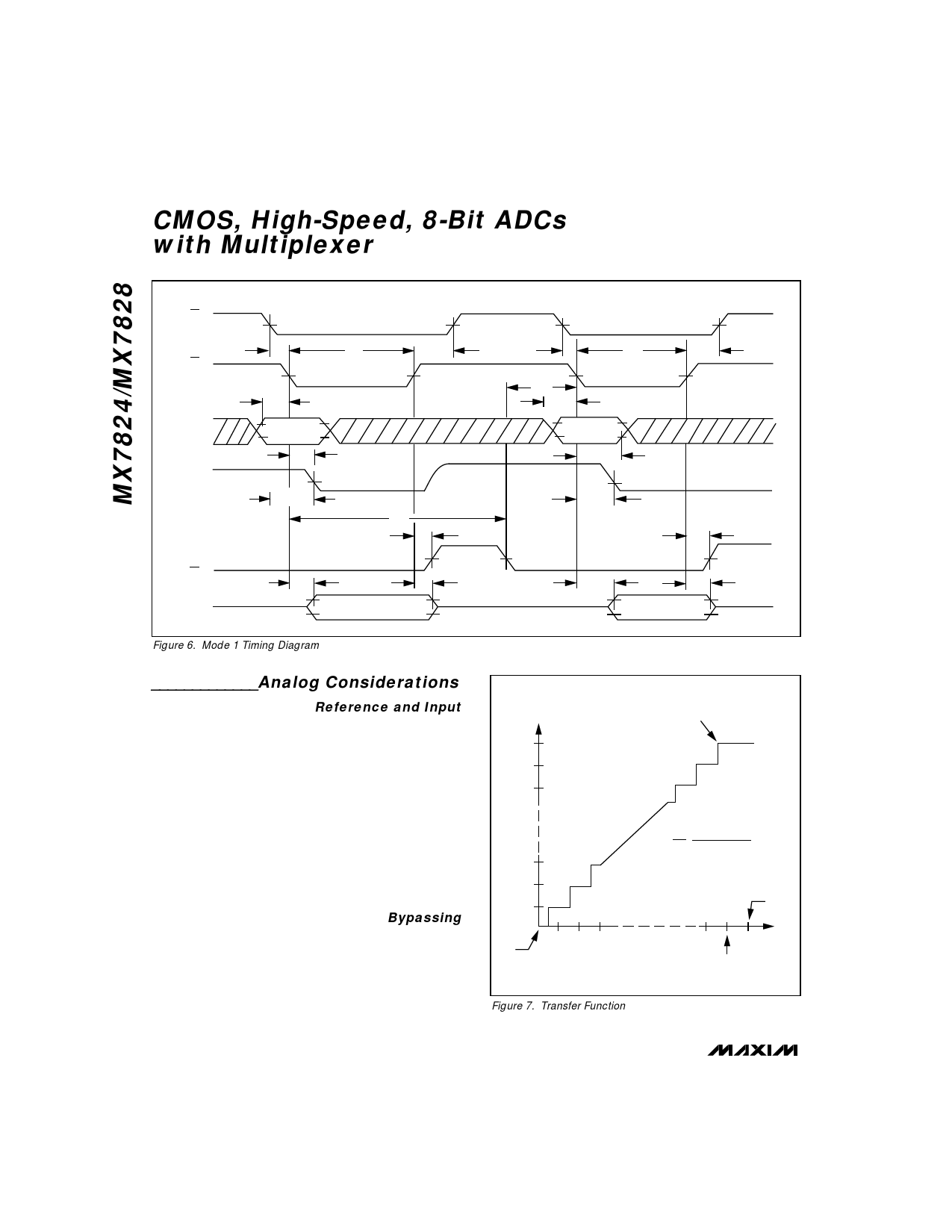
Figure 6. Mode 1 Timing Diagram
tDH
OLD
DATA
tACCI
tDH
NEW
DATA
_____________Analog Considerations
Reference and Input
The VREF+ and VREF- inputs of the converter define the
zero and the full-scale of the ADC. In other words, the
voltage at VREF- is equal to the input voltage that pro-
duces an output code of all zeros, and the voltage at
VREF+ is equal to input voltage that produces an output
code of all ones (Figure 7).
Figure 8 shows some possible reference configura-
tions. For the MAX154/MAX158, a 0.01µF bypass
capacitor to GND should be used to reduce the high-
frequency output impedance of the internal reference.
Larger capacitors should not be used, as this degrades
the stability of the reference buffer. The 2.5V reference
output is with respect to the GND pin.
Bypassing
A 47µF electrolytic and 0.1µF ceramic capacitor should
be used to bypass the VDD pin to GND. These capaci-
tors must have minimum lead length, since excess lead
length may contribute to conversion errors and instability.
If the reference inputs are driven by long lines, they
should be bypassed to GND with 0.1µF capacitors at
the reference input pins.
OUTPUT
CODE
11111111
11111110
11111101
FULL-SCALE
TRANSITION
00000011
00000010
00000001
00000000
VREF-
1LSB = F8 = VREF+ - VREF-
256
256
VREF+
123
AIN INPUT VOLTAGE
(IN TERMS OF LSBs)
FS
FS–1LSB
Figure 7. Transfer Function
8 _______________________________________________________________________________________