MX7828KCAI データシートの表示(PDF) - Maxim Integrated
部品番号
コンポーネント説明
一致するリスト
MX7828KCAI Datasheet PDF : 12 Pages
| |||
CMOS, High-Speed, 8-Bit ADCs
with Multiplexer
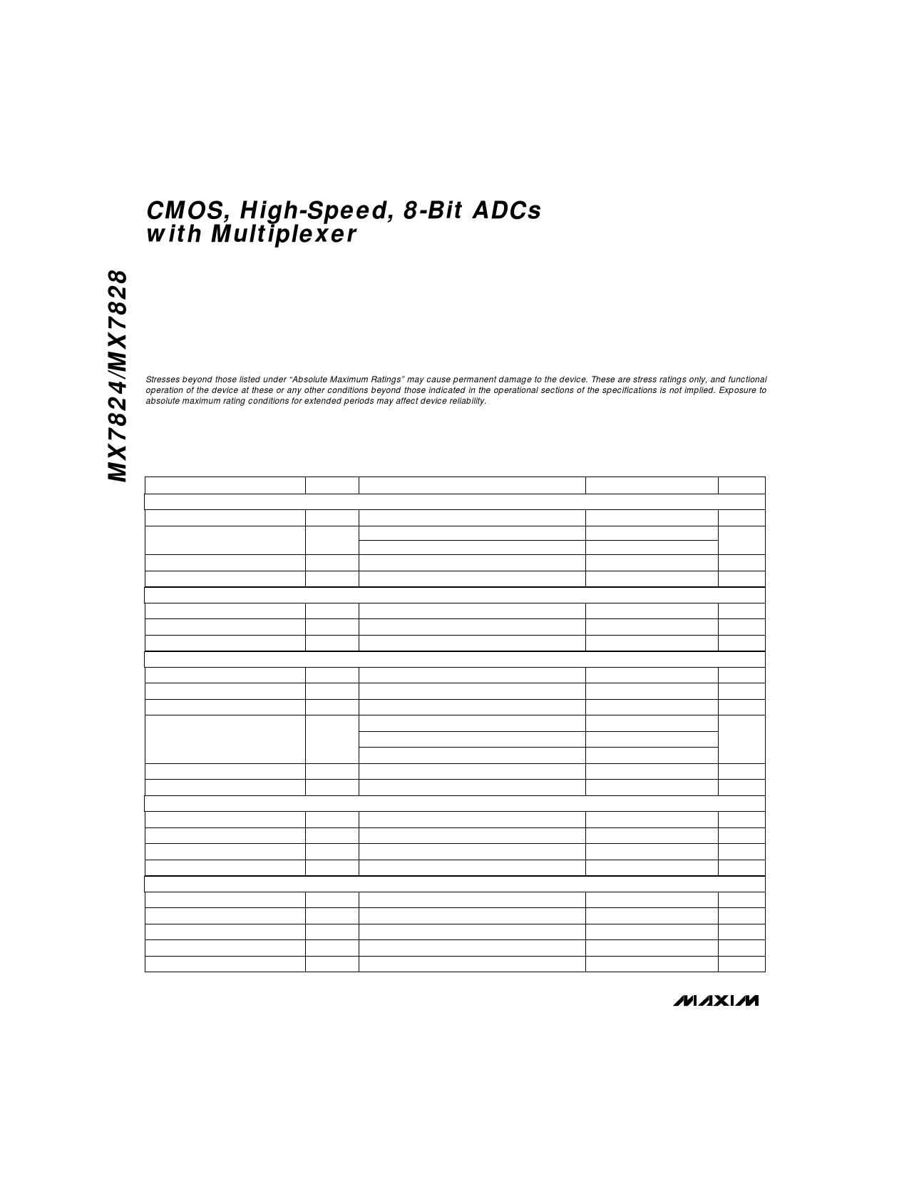
ABSOLUTE MAXIMUM RATINGS
Supply Voltage, VDD to GND ........................................0V, +10V
Voltage at Any Other Pins......................GND - 0.3V, VDD + 0.3V
Output Current (REF OUT)..................................................30mA
Power Dissipation (any package) to +75°C ....................450mW
Derate above +25°C by ..............................................6mW/°C
Operating Temperature Ranges
MX7824, MX7828
KN/LN/KCW_/LCW_ ............................................0°C to +70°C
BQ/CQ .............................................................-40°C to +85°C
TQ/UQ............................................................-55°C to +125°C
Storage Temperature Range .............................-65°C to +160°C
Lead Temperature (soldering, 10sec) .............................+300°C
Stresses beyond those listed under “Absolute Maximum Ratings” may cause permanent damage to the device. These are stress ratings only, and functional
operation of the device at these or any other conditions beyond those indicated in the operational sections of the specifications is not implied. Exposure to
absolute maximum rating conditions for extended periods may affect device reliability.
ELECTRICAL CHARACTERISTICS
(VDD = +5V, VREF+ = +5V, VREF- = GND, Mode 0, TA = TMIN to TMAX, unless otherwise noted.)
PARAMETER
SYMBOL
CONDITIONS
ACCURACY
Resolution
Total Unadjusted Error (Note 1)
MAX15_A, MX782_L/C/U
MAX15_B, MX782_K/B/T
No Missing Codes Resolution
Channel to Channel Mismatch
REFERENCE INPUT
Reference Resistance
VREF+ Input Voltage Range
VREF- Input Voltage Range
REFERENCE OUTPUT—MAX154/MAX158 Only (Note 2)
Output Voltage
REF OUT TA = +25°C
Load Regulation
IL = 0mA to 10mA, TA = +25°C
Power-Supply Sensitivity
VDD ±5%, TA = +25°C
MAX15_C
Temperature Drift (Note 3)
MAX15_E
MAX15_M
Output Noise
eN
Capacitive Load
ANALOG INPUT
Analog Input Voltage Range
AINR
Analog Input Capacitance
CAIN
Analog Input Current
IAIN Any channel, AIN = 0V to 5V
Slew Rate, Tracking
SR
LOGIC INPUTS (–R—D–, –C—S–, A0, A1, A2)
Input High Voltage
VINH
Input Low Voltage
VINL
Input High Current
IINH
Input Low Current
IINL
Input Capacitance (Note 4)
CIN
MIN TYP MAX UNITS
8
Bits
±1/2
LSB
±1
8
Bits
±1/4 LSB
1
VREF-
GND
4
kΩ
VDD
V
VREF+
V
2.47 2.50 2.53
V
-6
-10
mV
±1
±3
mV
40
70
40
70 ppm/°C
60
100
200
µV/rms
0.01
µF
VREF-
VREF+
V
45
pF
±3
µA
0.7 0.157 V/µs
2.4
V
0.8
V
1
µA
-1
µA
5
8
pF
2 _______________________________________________________________________________________
Share Link: 