HB54A5129F1-10B データシートの表示(PDF) - Elpida Memory, Inc
部品番号
コンポーネント説明
一致するリスト
HB54A5129F1-10B Datasheet PDF : 16 Pages
| |||
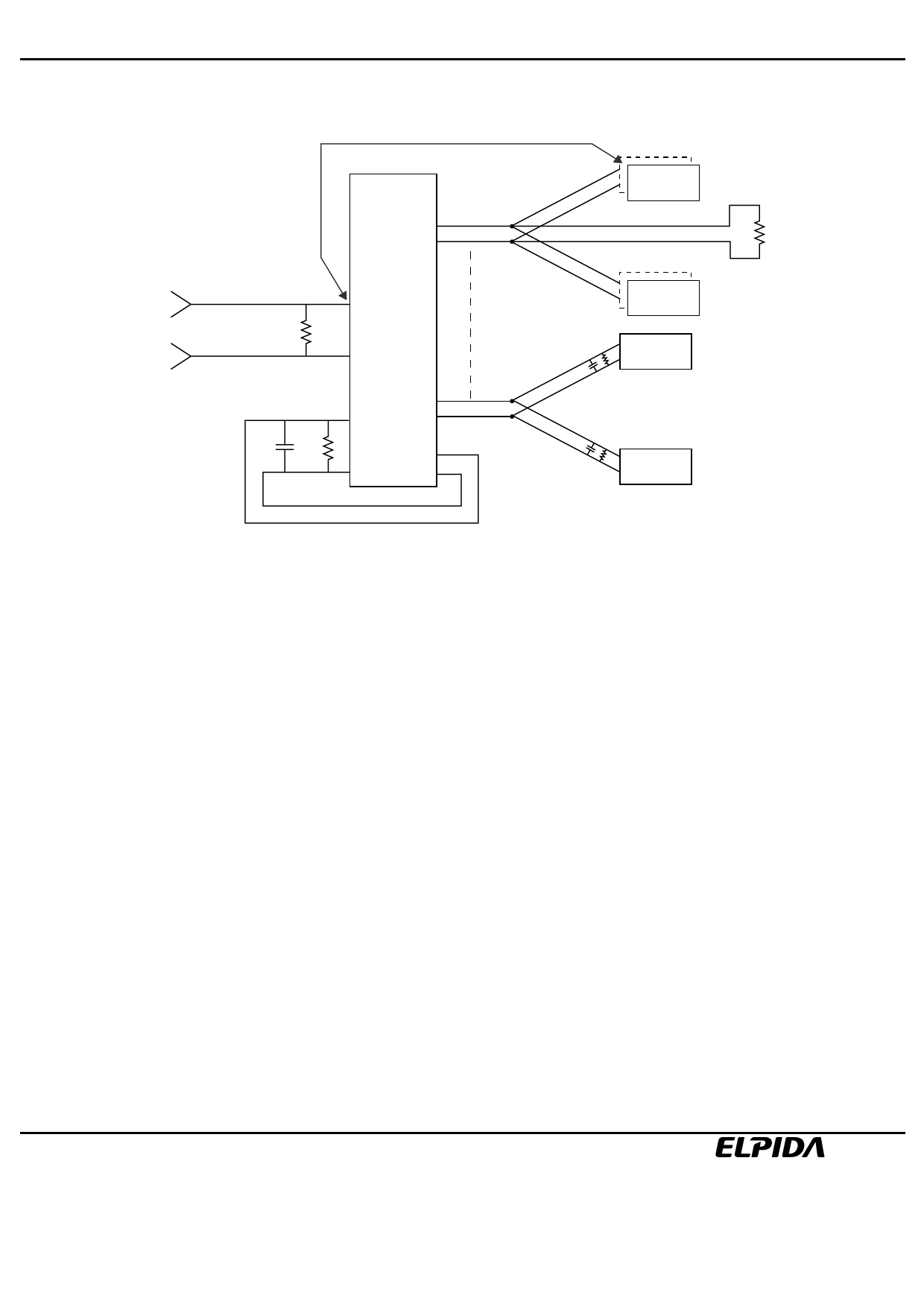
Differential Clock Net Wiring (CK0, /CK0)
0ns (nominal)
PLL
OUT1
CK0
/CK0
120Ω
IN
120Ω
OUT'N'
C
Feedback
HB54A5129F1-A75B/B75B/10B
SDRAM
stack
120Ω
SDRAM
stack
240Ω Register1
(Typically two registers per DIMM)
240Ω Register2
Notes: 1. The clock delay from the input of the PLL clock to the input of any SDRAM or register willl
be set to 0 ns (nominal).
2. Input, output and feedback clock lines are terminated from line to line as shown, and not
from line to ground.
3. Only one PLL output is shown per output type. Any additional PLL outputs will be wired
in a similar manner.
4. Termination resistors for feedback path clocks are located after the pins of the PLL.
Data Sheet E0090H40 (Ver. 4.0)
9
Share Link: 