CY7C1329-60AC データシートの表示(PDF) - Cypress Semiconductor
部品番号
コンポーネント説明
一致するリスト
CY7C1329-60AC Datasheet PDF : 14 Pages
| |||
CY7C1329
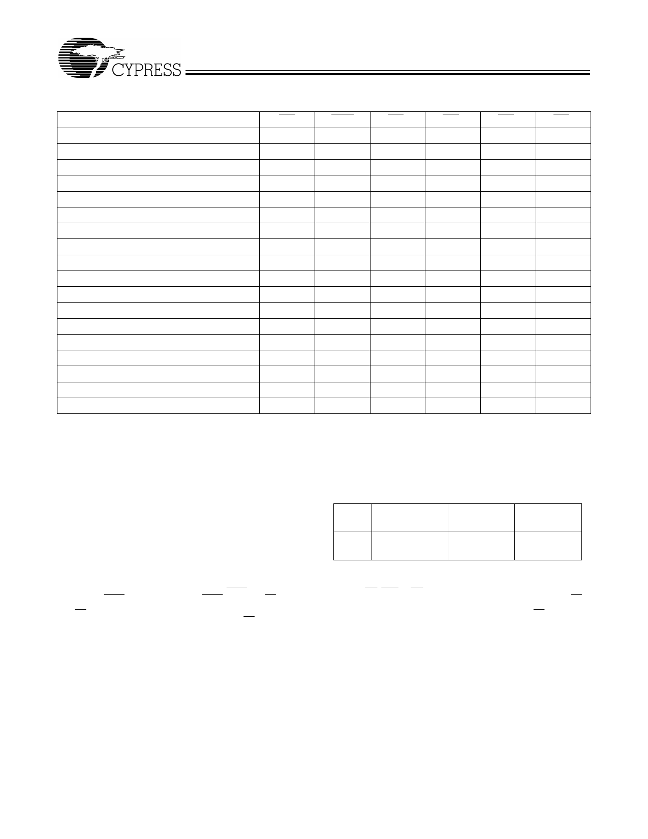
Write Cycle Descriptions[4,5,6]
Function
Read
Read
Write Byte 0 - DQ[7:0]
Write Byte 1 - DQ[15:8]
Write Bytes 1, 0
Write Byte 2 - DQ[23:16]
Write Bytes 2, 0
Write Bytes 2, 1
Write Bytes 2, 1, 0
Write Byte 3 - DQ[31:24]
Write Bytes 3, 0
Write Bytes 3, 1
Write Bytes 3, 1, 0
Write Bytes 3, 2
Write Bytes 3, 2, 0
Write Bytes 3, 2, 1
Write All Bytes
Write All Bytes
GW
BWE
BW3
BW2
BW1
BW0
1
1
X
X
X
X
1
0
1
1
1
1
1
0
1
1
1
0
1
0
1
1
0
1
1
0
1
1
0
0
1
0
1
0
1
1
1
0
1
0
1
0
1
0
1
0
0
1
1
0
1
0
0
0
1
0
0
1
1
1
1
0
0
1
1
0
1
0
0
1
0
1
1
0
0
1
0
0
1
0
0
0
1
1
1
0
0
0
1
0
1
0
0
0
0
1
1
0
0
0
0
0
0
X
X
X
X
X
Maximum Ratings
Current into Outputs (LOW)......................................... 20 mA
(Above which the useful life may be impaired. For user guide-
lines, not tested.)
Storage Temperature ..................................... −65°C to +150°C
Static Discharge Voltage .......................................... >2001V
(per MIL-STD-883, Method 3015)
Latch-Up Current .................................................... >200 mA
Ambient Temperature with
Power Applied .................................................. −55°C to +125°C
Supply Voltage on VDD Relative to GND .........−0.5V to +4.6V
DC Voltage Applied to Outputs
in High Z State[7] .....................................−0.5V to VDDQ + 0.5V
DC Input Voltage[7]..................................−0.5V to VDDQ + 0.5V
Operating Range
Ambient
Range Temperature[8]
Com’l 0°C to +70°C
VDD
3.3V
−5%/+10%
VDDQ
3.3V
−5%/+10%
Notes:
4. X=”Don't Care”, 1=Logic HIGH, 0=Logic LOW.
5. The SRAM always initiates a read cycle when ADSP asserted, regardless of the state of GW, BWE, or BW[3:0]. Writes may occur only on subsequent clocks
after the ADSP or with the assertion of ADSC. As a result, OE must be driven HIGH prior to the start of the write cycle to allow the outputs to three-state. OE is
a “don't care” for the remainder of the write cycle.
6. OE is asynchronous and is not sampled with the clock rise. It is masked internally during write cycles. During a read cycle DQ=High-Z when OE is inactive or
when the device is deselected, and DQ=data when OE is active.
7. Minimum voltage equals –2.0V for pulse durations of less than 20 ns.
8. TA is the case temperature.
6
Share Link: 