MSM7716PMB データシートの表示(PDF) - Oki Electric Industry
部品番号
コンポーネント説明
一致するリスト
MSM7716PMB Datasheet PDF : 23 Pages
| |||
OKI Semiconductor
FEDL7716P-01
MSM7716P
DEN, DCLK, CDIN
Serial control ports for the microcontroller interface.
Writing data to the 8-bit control register enables control of the receive output level and the signal path.
DEN is the “Enable” signal pin, DCLK is the data shift clock input pin, and CDIN is the control data input pin.
When powered down (PDN = 0), the initial values are set as shown in Tables 2, 3, and 4. The initial values are held
unless the control data is written after power-down release.
The control data is shifted at the rising edge of the DCLK signal and latched into the internal control register at the
rising edge of the DEN signal.
When the microcontroller interface is not used, these pins should be connected to DG.
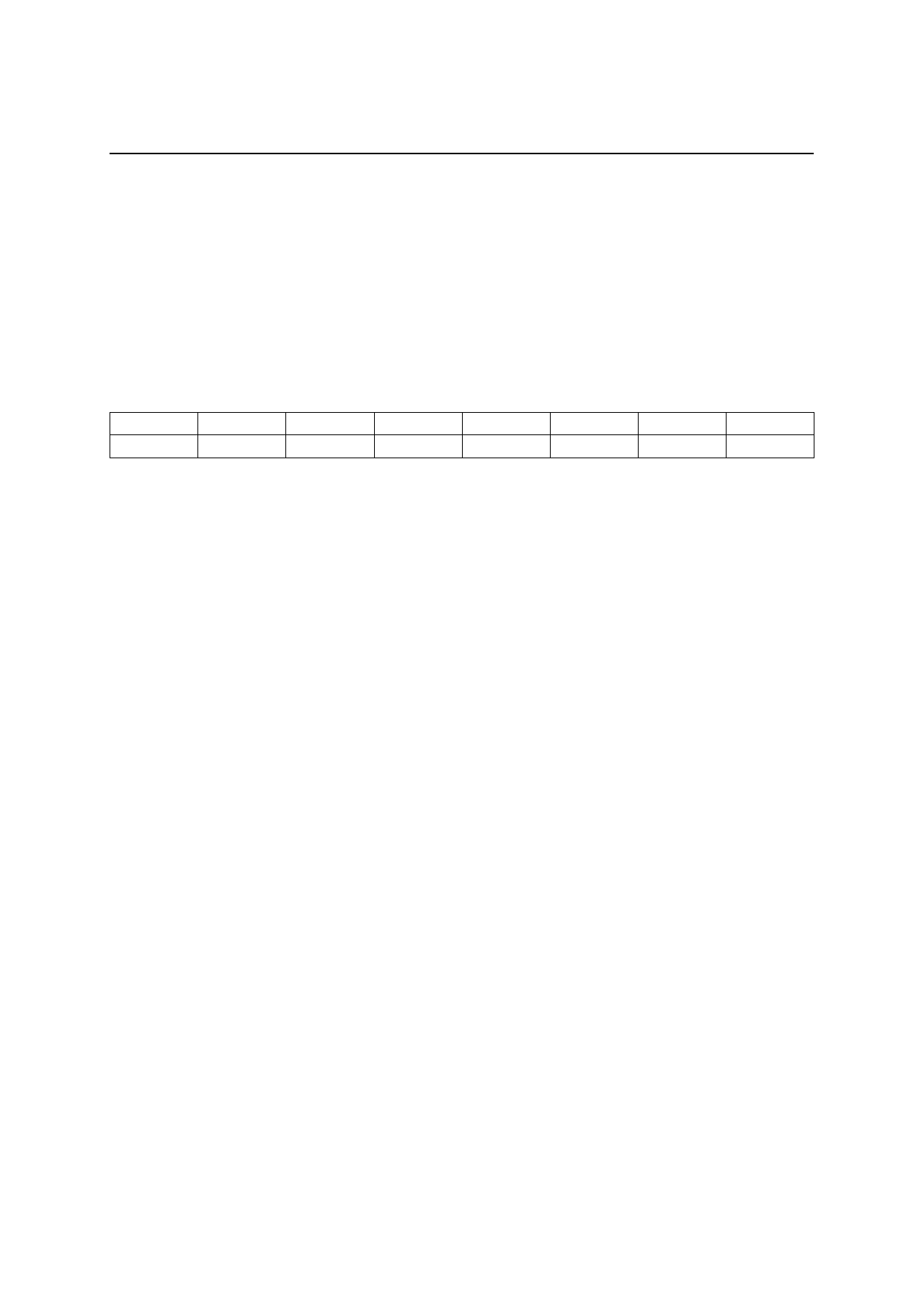
The bit map of the 8-bit control register is shown below.
B7
SW1
B6
SW2
B5
SW3
B4
SW4
B3
B2
B1
B0
—
VOL1
VOL2
VOL3
8/23
Share Link: 