MSM7716PMB データシートの表示(PDF) - Oki Electric Industry
部品番号
コンポーネント説明
一致するリスト
MSM7716PMB Datasheet PDF : 23 Pages
| |||
OKI Semiconductor
FEDL7716P-01
MSM7716P
PIN AND FUNCTIONAL DESCRIPTIONS
MAIN, MAO
Transmit microphone input and the level adjustment.
MAIN is connected to the noninverting input of the op-amp, and MAO is connected to the output of the op-amp.
The level adjustment should be configured as shown below.
During power saving and power down modes, the MAO output is in high impedance state.
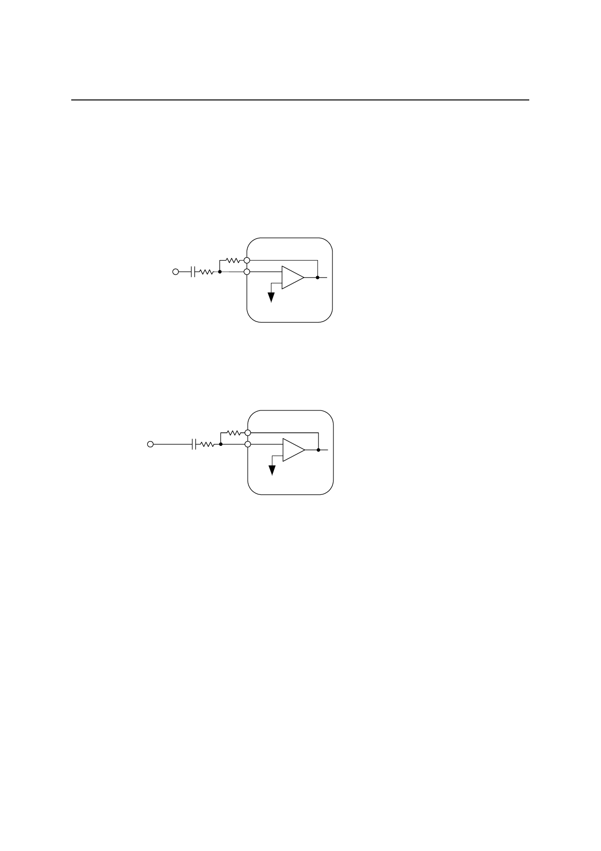
Microphone input
MAO
C1
R2 MAIN –
R1
+
SG
R1 : variable
R2 > 20 kΩ
C1 > 1/ (2 × 3.14 × 30 × R3) (F)
Gain = R2/R1 < 63
PBIN, PBO
Transmit handset input and the level adjustment.
PBIN is connected to the noninverting input of the op-amp, and PBO is connected to the output of the op-amp. The
level adjustment should be configured as shown below.
During power saving and power down, the PBO output is in high impedance state.
Handset
microphone input
R4 PBO
C2
PBIN –
R3
+
SG
R3 : variable
R4 > 20 kΩ
C2 > 1/ (2 × 3.14 × 30 × R3) (F)
Gain = R4/R3 < 63
VDD
Power supply pin for +3.0 to 3.6 V (Typically 3.3 V).
AG
Analog signal ground.
DG
Ground pin for the digital signal circuits.
This ground is separated from the analog signal ground in this device. The DG pin must be connected to the AG pin
on the printed circuit board.
4/23
Share Link: 