MC74HC74AFL1 データシートの表示(PDF) - ON Semiconductor
部品番号
コンポーネント説明
一致するリスト
MC74HC74AFL1 Datasheet PDF : 9 Pages
| |||
MC74HC74A
Dual D Flip-Flop with Set
and Reset
High−Performance Silicon−Gate CMOS
The MC74HC74A is identical in pinout to the LS74. The device
inputs are compatible with standard CMOS outputs; with pullup
resistors, they are compatible with LSTTL outputs.
This device consists of two D flip−flops with individual Set, Reset,
and Clock inputs. Information at a D−input is transferred to the
corresponding Q output on the next positive going edge of the clock
input. Both Q and Q outputs are available from each flip−flop. The Set
and Reset inputs are asynchronous.
Features
• Output Drive Capability: 10 LSTTL Loads
• Outputs Directly Interface to CMOS, NMOS, and TTL
• Operating Voltage Range: 2.0 to 6.0 V
• Low Input Current: 1.0 mA
• High Noise Immunity Characteristic of CMOS Devices
• In Compliance with the JEDEC Standard No. 7.0 A Requirements
• Chip Complexity: 128 FETs or 32 Equivalent Gates
• These Devices are Pb−Free, Halogen Free and are RoHS Compliant
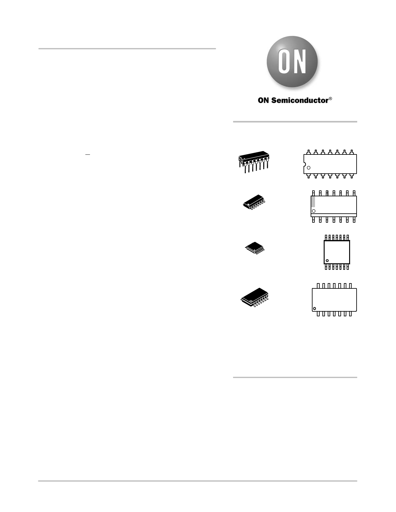
http://onsemi.com
14
1
14
1
MARKING
DIAGRAMS
14
PDIP−14
N SUFFIX
CASE 646
1
MC74HC74AN
AWLYYWWG
14
SOIC−14
D SUFFIX
CASE 751A
1
HC74AG
AWLYWW
14
1
TSSOP−14
DT SUFFIX
CASE 948G
14
HC
74A
ALYWG
G
1
14
14
1
SOEIAJ−14
F SUFFIX
CASE 965
74HC74A
ALYWG
1
A
L, WL
Y, YY
W, WW
G or G
= Assembly Location
= Wafer Lot
= Year
= Work Week
= Pb−Free Package
(Note: Microdot may be in either location)
ORDERING INFORMATION
See detailed ordering and shipping information in the package
dimensions section on page 4 of this data sheet.
© Semiconductor Components Industries, LLC, 2011
1
May, 2011 − Rev. 12
Publication Order Number:
MC74HC74A/D
Share Link: 