MC74HC365A(2019) データシートの表示(PDF) - ON Semiconductor
部品番号
コンポーネント説明
一致するリスト
MC74HC365A Datasheet PDF : 8 Pages
| |||
MC74HC365A
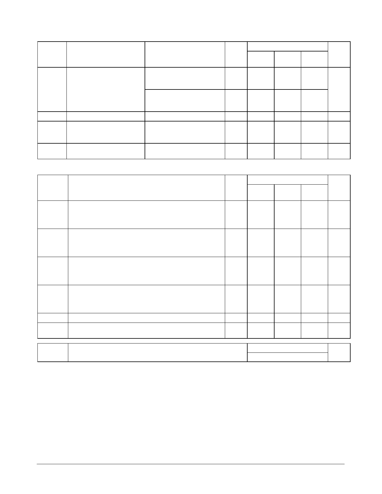
DC ELECTRICAL CHARACTERISTICS (Voltages Referenced to GND)
Guaranteed Limit
Symbol
Parameter
Test Conditions
VCC
– 55 to
V
25_C v 85_C v 125_C Unit
Iin
Maximum Input Leakage Current Vin = VCC or GND
6.0
± 0.1
± 1.0
± 1.0
μA
IOZ
Maximum Three−State
Leakage Current
Output in High−Impedance State
6.0
± 0.5
± 5.0
± 10
μA
Vin = VIL or VIH
Vout = VCC or GND
ICC
Maximum Quiescent Supply
Current (per Package)
Vin = VCC or GND
Iout = 0 μA
6.0
4
40
160
μA
AC ELECTRICAL CHARACTERISTICS (CL = 50 pF, Input tr = tf = 6 ns)
Symbol
tPLH,
tPHL
Parameter
Maximum Propagation Delay, Input A to Output Y
(Figures 1 and 3)
tPLZ,
tPHZ
Maximum Propagation Delay, Output Enable to Output Y
(Figures 2 and 4)
tPZL,
tPZH
Maximum Propagation Delay, Output Enable to Output Y
(Figures 2 and 4)
tTLH,
tTHL
Maximum Output Transition Time, Any Output
(Figures 1 and 3)
Cin
Maximum Input Capacitance
Cout
Maximum Three−State Output Capacitance
(Output in High−Impedance State)
Guaranteed Limit
VCC
– 55 to
V
25_C v 85_C v 125_C Unit
2.0
120
150
180
ns
3.0
60
75
90
4.5
24
30
36
6.0
20
26
31
2.0
220
275
330
ns
3.0
110
140
170
4.5
44
55
66
6.0
37
47
56
2.0
220
275
330
ns
3.0
110
140
170
4.5
44
55
66
6.0
37
47
56
2.0
60
75
90
ns
3.0
22
28
34
4.5
12
15
18
6.0
10
13
15
—
10
10
10
pF
—
15
15
15
pF
Typical @ 25°C, VCC = 5.0 V
CPD
Power Dissipation Capacitance (Per Buffer)*
60
pF
* Used to determine the no−load dynamic power consumption: PD = CPD VCC2f + ICC VCC.
SWITCHING WAVEFORMS
tr
INPUT A
tPLH
OUTPUT Y
90%
50%
10%
90%
50%
10%
tTLH
Figure 1.
tf
VCC
GND
tPHL
tTHL
OUTPUT ENABLE
OUTPUT Y
OUTPUT Y
50%
tPZL tPLZ
50%
tPZH tPHZ
50%
Figure 2.
VCC
GND
HIGH
IMPEDANCE
10% VOL
90% VOH
HIGH
IMPEDANCE
www.onsemi.com
4
Share Link: 