MB90520 データシートの表示(PDF) - Fujitsu
部品番号
コンポーネント説明
一致するリスト
MB90520 Datasheet PDF : 106 Pages
| |||
MB90520 Series
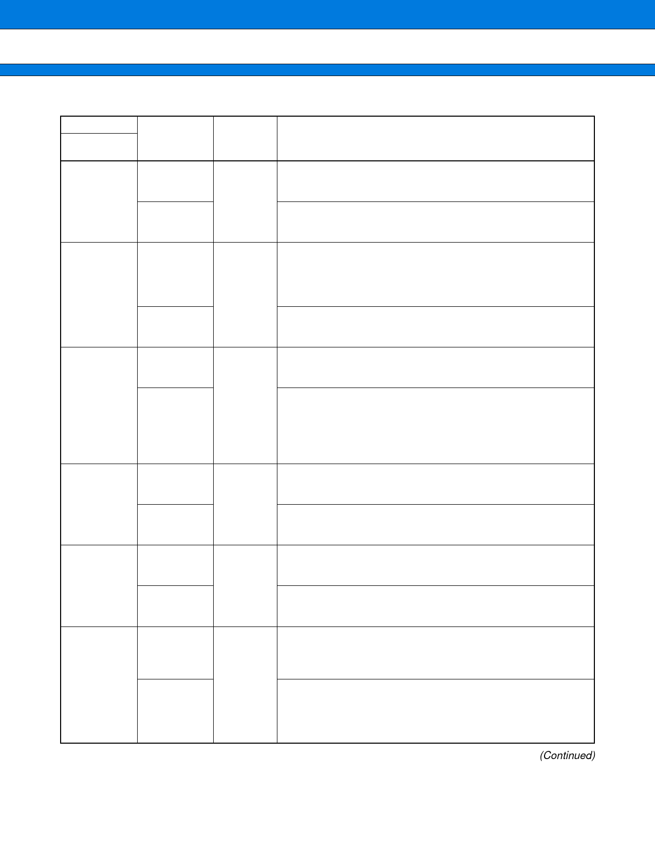
Pin no.
LQFP-120*1
QFP-120*2
7
Pin name
P37
PG01
9,
P40,
10
P41
PG10,
PG11
11
P42
SIN0
12
P43
SOT0
13
P44
SCK0
14
P45
SIN1
*1: FPT-120P-M05
*2: FPT-120P-M13
Circuit
type
Function
E
This is a general-purpose I/O port.
This function becomes valid when waveform output from the PG01
is disabled.
This is an output pin of 8/16-bit PPG timer 0.
This function becomes valid when waveform output from PG01 is
enabled.
D
This is a general-purpose I/O port.
This function becomes valid when waveform output from the PG10
and PG11 are disabled.
This function can be set by the pull-up resistor setup register
(RDR4) for input. For output, however, this function is invalid.
This is an output pin of 8/16-bit PPG timer 1.
This function becomes valid when waveform outputs from PG10
and PG11 are enabled.
D
This is a general-purpose I/O port.
This function can be set by the pull-up resistor setup register
(RDR4) for input. For output, however, this function is invalid.
This is a serial data input pin of UART (SCI).
Because this input is used as required when UART (SCI) is
performing input operations, it is necessary to stop outputs by
other functions unless such outputs are made intentionally.
When using other output functions as well, disable output during
SIN operation.
D
This is a general-purpose I/O port.
This function can be set by the pull-up resistor setup register
(RDR4) for input. For output, however, this function is invalid.
This is a serial data output pin of UART (SCI).
This function becomes valid when serial data output from UART
(SCI) is enabled.
D
This is a general-purpose I/O port.
This function can be set by the pull-up resistor setup register
(RDR4) for input. For output, however, this function is invalid.
This is a serial clock I/O pin of UART (SCI).
This function becomes valid when serial clock output from UART
(SCI) is enabled.
D
This is a general-purpose I/O port.
This function can be set by the port 4 input pull-up resistor setup
register (RDR4) for input. For output, however, this function is
invalid.
This is a data input pin for extended I/O serial interface 0.
Since this input is used as required for serial data input operation,
output by other functions must be suspended except for intentional
operation. When using other output functions as well, disable
output during SIN operation.
(Continued)
10
Share Link: 