LX8821CDF データシートの表示(PDF) - Microsemi Corporation
部品番号
コンポーネント説明
一致するリスト
LX8821CDF Datasheet PDF : 6 Pages
| |||
LX8821
TM
®
DUAL CHANNEL 2.5A LOW DROPOUT REGULATOR
PRODUCTION DATA SHEET
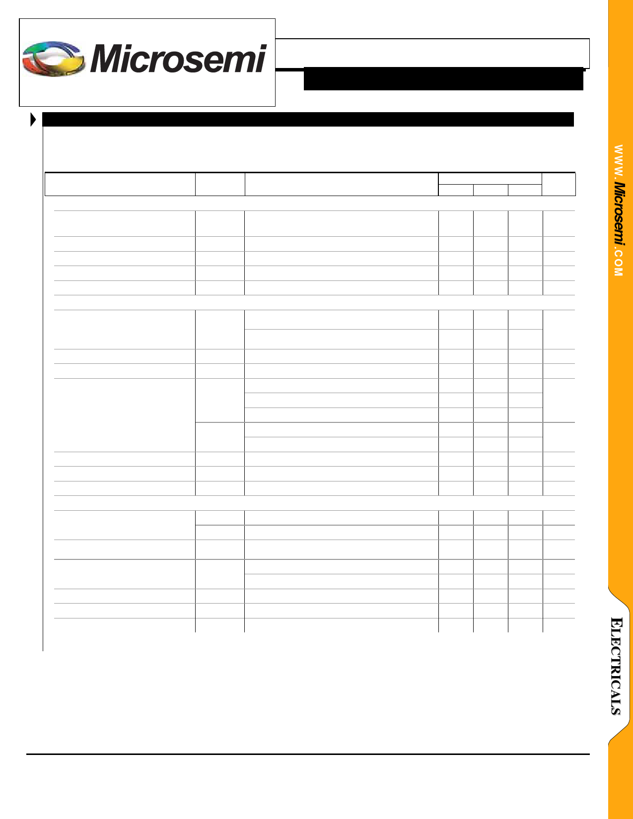
ELECTRICAL CHARACTERISTICS
Unless otherwise specified, the following specifications apply over the operating ambient temperature 0°C ≤ TA ≤ 100°C except where
otherwise noted and the following test conditions: VCTRL = 5V, VPWR = 3.3V IOUT = 5mA, C1, 2, 3, 4 = 10μF (Tantalum), and TJ = TA using
low duty cycling methods. Typical values represent performance @ 23°C
Parameter
` FIXED OUTPUT: VOUT 1
Total Output Voltage Variation
Line Regulation
Load Regulation
Current Limit
Minimum Load Current
` ADJUSTABLEOUTPUT: VOUT 2
Output Voltage
Line Regulation
Load Regulation
Dropout Voltage, VOUT 2
Adjust Pin Current
Current Limit
Minimum Load Current
` ENTIRE REGULATOR
Minimum Operating Voltage
Under Voltage Lockout
Quiescent Current
Ripple Rejection
RMS Output Noise
Thermal Shutdown
Symbol
Test Conditions
V1
ΔV1(VIN)
ΔV1(I1)
I1 (MAX)
I1
5mA < I1 < 2.5A, 3.75V < VCTRL < 8V
3.3V < VPWR < 5.5V
3.3V<VCTRL<10V, 3.3V<VPWR<5.5V, I1 = 5mA
5mA < I1 < 2.5A, VCTRL=5V, VPWR=3.3V
Note 1
V2
ΔV2(VIN)
ΔV2(I2)
VPWR-V2
VCNTR-V2
I2 (MAX)
I2
5mA < I2 < 2.5A, 3.75V < VCTRL < 8V
2.97V < VPWR < 3.63V
5mA < I2 < 2.5A, 3.75V < VCTRL < 8V,
3.3V < VPWR < 5.5V
3.3V<VCTRL<10V, 3.3V<VPWR<5.5V, I2 = 5mA
5mA < I2 < 2.5A, VCTRL=5V, VPWR=3.3V
IOUT = 2.5A, ∆VO = -2%
IOUT = 2.0A, ∆VO = -2%
IOUT = 1.0A, ∆VO = -2%
IOUT = 2.5A, ∆VO = -2%
IOUT = 1.0A, ∆VO = -2%
I1 = I2 = 5mA, TJ = 25°C
Note 1
VPWR
VCONTROL
IQ
PSRR
TJSD
VPWR Rising, 3.0V<VCTRL < 10V, Both Outputs
Guaranteed Off
I1=I2=5mA
I1 = I2 = 2.5A
f=120Hz, TJ = 25°C
10Hz < f < 10kHz
LX8821
Units
Min Typ Max
1.455 1.500 1.545 V
1
1
2.55
3.0
0
5
mV
5
mV
A
5
mA
1.225 1.25 1.275
V
1.225 1.25 1.288
0.5
5
mV
8
20
mV
0.500 0.750
0.413 0.600 V
0.167 0.400
0.95 1.10
V
0.80 1.00
0.2
1
µA
2.55
3.0
A
1
5
mA
2.6
V
3.3
V
2.2
V
3
5
mA
5
10
mA
60
75
dB
0.003
160
%VOUT
°C
Note 1: Minimum load current is defined as the amount of output current required to maintain regulation
Copyright © 2005
Rev. 1.1, 2005-03-09
Microsemi
Microsemi Microelectronics Division
11861 Western Avenue, Garden Grove, CA. 92841, 714-898-8121, Fax: 714-893-2570
Page 3
Share Link: 