LX8821CDF データシートの表示(PDF) - Microsemi Corporation
部品番号
コンポーネント説明
一致するリスト
LX8821CDF Datasheet PDF : 6 Pages
| |||
LX8821
TM
®
DUAL CHANNEL 2.5A LOW DROPOUT REGULATOR
PRODUCTION DATA SHEET
ABSOLUTE MAXIMUM RATINGS
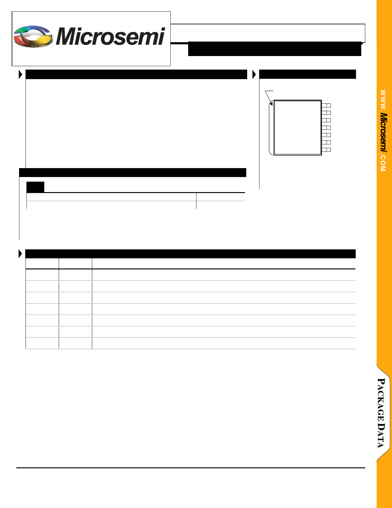
PACKAGE PIN OUT
Input Voltage (VCTRL, VPWR).........................................................................13.5V
Load Current (Internally Limited) ..................................................................3.0A
Power Dissipation ......................................................................Internally Limited
Short-Circuit Protection .......................................................................... Indefinite
Operating Junction Temperature.................................................................. 150°C
Storage Temperature Range...........................................................-65°C to 150°C
Peak Package Solder Reflow Temperature
(40 second maximum exposure) ..................................................... 260°C (+0, -5)
Note: Exceeding these ratings could cause damage to the device. All voltages are with respect to
Ground. Currents are positive into, negative out of specified terminal.
THERMAL DATA
DF Plastic S-Pak 7-Pin
THERMAL RESISTANCE-JUNCTION TO TAB, θJT
THERMAL RESISTANCE-JUNCTION TO AMBIENT, θJA
4.5°C/W
20 - 50°C/W
Junction Temperature Calculation: TJ = TA + (PD x θJA).
The θJA numbers are guidelines for the thermal performance of the device/pc-board system.
All of the above assume no ambient airflow. θJA can vary from 10°C/W to > 50°C/W
depending on mounting technique. (See Application Notes Section: Thermal considerations)
TAB is GND
7
NC
6
ADJV2
5
V O UT2
4
GND
3
VPWR
2
V O UT1
1
V C TR L
DF PACKAGE
(Top View)
Pin 4 and Tab are common
RoHS 100% Matte Tin Lead Finish
PIN
NAME
FUNCTIONAL PIN DESCRIPTION
DESCRIPTION
1
VCTRL
Unregulated input voltage supply, provides bias for control circuitry, (VCTRL – VOUT) > 1V.
2
VOUT1
Regulator #1 fixed output voltage, 1.5V nominal.
3
VPWR
Unregulated input voltage supply for power section. For proper operation: (VPWR – VOUT) > VDROPOUT.
4
GND
Common terminal for ground reference, Tab of package is internally connected to this pin.
5
VOUT2
Regulator #2 output
6
ADJ V2
Regulator #2 feedback voltage, servos to 1.25V. Using external resistors to program VOUT2.
7
---
Not used, no internal connection, may be left floating or connected to any other pin or voltage.
Copyright © 2005
Rev. 1.1, 2005-03-09
Microsemi
Microsemi Microelectronics Division
11861 Western Avenue, Garden Grove, CA. 92841, 714-898-8121, Fax: 714-893-2570
Page 2
Share Link: 