L6382D5 データシートの表示(PDF) - STMicroelectronics
部品番号
コンポーネント説明
一致するリスト
L6382D5 Datasheet PDF : 21 Pages
| |||
L6382D5
Electrical characteristics
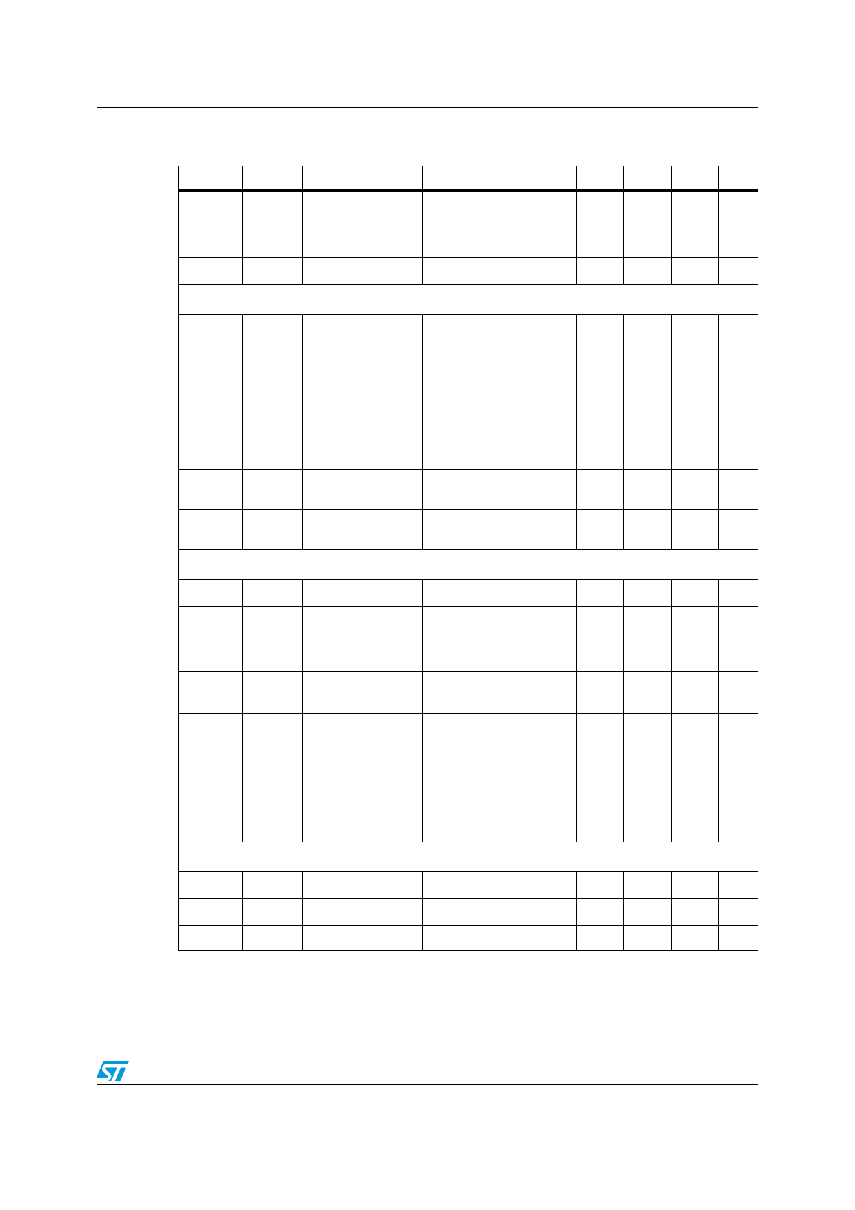
Table 4. Electrical characteristcs (TJ = 25°C, VCC = 13V, CDRIVER = 1nF
unless otherwise specified) (continued)
Symbol Pin
Parameter
Test condition
Min Typ
TFALL
12 Fall time
Cload = 1nF
75
TDELAY
12
Propagation delay high to low and low to
(LGI to LSG)
high
RB
12 Pull down Resistor to OUT
20
High-side floating gate-driver supply
ILKBOOT
ILKOUT
RDS(on)
11
VBOOT pin leakage
current
VBOOT = 580V
13
OUT pin leakage
current
VOUT = 562V
Synchronous
bootstrap
diode on-
VLVG = HIGH
150
resistance
Forward Voltage
Drop
at 10 mA forward current
2.4
Forward Current
at 5V forward voltage
drop
20
VREF
VREF
IREF
20 Reference voltage 15mA load.
4.9
5
20 Load regulation IRef = -3 to +30 mA
-20
20 Voltage change
15mA load; Vcc = 9V to
15V
20
VREF latched
protection
VCC from 0 to VCCON
20
VREF Clamp
@3mA
during start-up; Vcc from
VREF(OFF) to 0 during
1.2
shut-down; VREF < 2V
20
Current Drive
Capability
Save mode
-3
-3
Overcurrent buffer stage
VCSI
ICSI
19 Comparator Level
0.52 0.54
19 Input Bias Current
Propagation delay CSO turn off to LSG low
Max Unit
ns
300 ns
KΩ
5 µA
5 µA
Ω
V
mA
5.1 V
2 mV
15 mV
3.2 V
1.8 V
+30 mA
+10 mA
0.56 V
500 nA
200 ns
9/21
Share Link: 