L6382D5 データシートの表示(PDF) - STMicroelectronics
部品番号
コンポーネント説明
一致するリスト
L6382D5 Datasheet PDF : 21 Pages
| |||
L6382D5
Pin settings
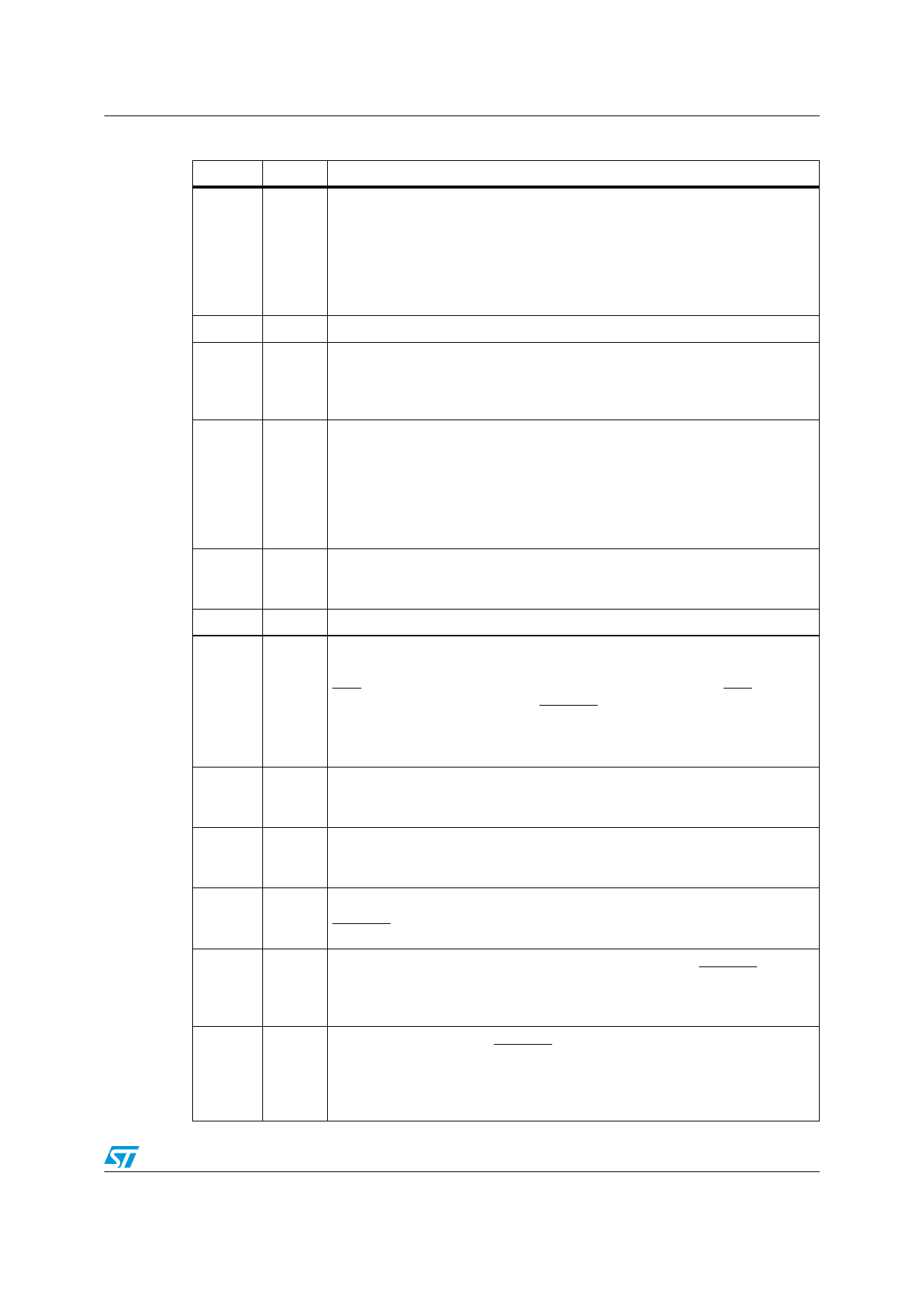
Table 1. Pin description (continued)
Name Pin N°
Description
Low Side Driver Output. This pin must be connected to the gate of the half-
bridge low side power MOSFET. A resistor connected between this pin and the
power MOS gate can be used to reduce the peak current.
9
LSG An internal 20KΩ resistor toward ground avoids spurious and undesired
MOSFET turn-on.
The totem pole output stage is able to drive power with a peak current of
120mA source and 120mA sink.
10
Vcc Supply Voltage for the signal part of the IC and for the drivers.
High-side gate-drive floating supply Voltage. The bootstrap capacitor
11
BOOT
connected between this pin and pin 13 (OUT) is fed by an internal
synchronous bootstrap diode driven in phase with the low-side gate-drive. This
patented structure normally replaces the external diode.
High Side Driver Output. This pin must be connected to the gate of the half
bridge high side power MOSFET . A resistor connected between this pin and
the power MOS gate can be used to reduce the peak current.
12
HSG An internal 20KΩ resistor toward OUT pin avoids spurious and undesired
MOSFET turn-on
The totem pole output stage is able to drive the power MOS with a peak
current of 120mA source and 120mA sink.
High-side gate-drive floating ground. Current return for the high-side gate-drive
13
OUT current. Layout carefully the connection of this pin to avoid too large spikes
below ground.
14
N.C. Not connected
High-voltage start-up. The current flowing into this pin charges the capacitor
connected between pin Vcc and GND to start up the IC. Whilst the chip is in
save mode, the generator is cycled on-off between turn-on and save mode
15
HVSU voltages. When the chip works in operating mode the generator is shut down
and it is re-enabled when the Vcc voltage falls below the UVLO threshold.
According to the required VREF pin current, this pin can be connected to the
rectified mains voltage either directly or through a resistor.
High-voltage spacer. The pin is not connected internally to isolate the high-
16
N.C. voltage pin and comply with safety regulations (creepage distance) on the
PCB.
Output for the HEI block; this driver can be used to drive the MOS employed in
17
HEG isolated filaments preheating. An internal 20KΩ resistor toward ground avoids
spurious and undesired MOSFET turn-on.
Output of current sense comparator, compatible with 5V CMOS logic; during
18
CSO operating mode, the pin is forced low whereas whenever the OC comparator is
triggered (CSI> 0.55 typ.) the pin latches high.
Input of current sense comparator, it is enabled only during operating mode;
19
CSI
when the pin voltage exceeds the internal threshold, the CSO pin is forced
high and the half bridge drivers are disabled. It exits from this condition by
either cycling the Vcc below the UVLO or with LGI=HGI=low simultaneously.
Voltage reference. During operating mode an internal generator provides an
accurate voltage reference that can be used to supply up to 30mA to an
20
VREF external circuit. A small film capacitor (0.22µF min.), connected between this
pin and GND is recommended to ensure the stability of the generator and to
prevent noise from affecting the reference.
5/21
Share Link: 