L6382DTR(2005) データシートの表示(PDF) - STMicroelectronics
部品番号
コンポーネント説明
一致するリスト
L6382DTR Datasheet PDF : 14 Pages
| |||
L6382D
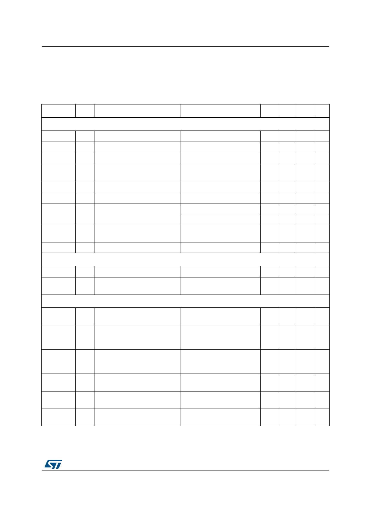
Table 5. Electrical Characteristcs (continued)
Symbol Pin
Parameter
Test condition
min. typ max UNIT
VREF
VREF
20 Reference voltage
15mA load.
15mA load, (1)
3.267 3.3 3.333 V
3.234 3.3 3.366 V
20 Load regulation
IRef = -3 to +30 mA
-20
2
mV
20 Voltage change
15mA load; Vcc = 9V to 15V
15
mV
20 VREF latched protection
2
V
20 VREF Clamp @3mA
VCC from 0 to VCCON during
start-up; Vcc from VREF(OFF) to
0 during shut-down.
1.2
V
IREF
20 Current Drive Capability
Save mode
-3
+30 mA
-3
+10 mA
OVERCURRENT BUFFER STAGE
VCSI
19 Comparator Level
Bandgap
0.49 0.5 5.01
V
ICSI
19 Input Bias Current
500
nA
Propagation delay
CSO turn off to LSG low
200
ns
18 High output voltage
I CSO= 200µA
VREF-
0.5V
18 Low output voltage
I CSO = -150µA
0.5
V
DIM
Normal Mode Time Out
65
100 135
µs
Vref enabling drivers
3.0
V
TED
Time enabling drivers
10
µs
LOGIC INPUT
1 to 4 Low Level Logic Input
Voltage
0.8
V
1 to 4 High Level Logic Input
Voltage
2.2
V
LGI Pull down resistor
100
KΩ
Notes: 1. Specification over the -40°C to +125°C junction temperature range are ensured by design, characterization and statistical corre-
lation.
7/14
Share Link: 