IDT7024 データシートの表示(PDF) - Integrated Device Technology
部品番号
コンポーネント説明
一致するリスト
IDT7024 Datasheet PDF : 22 Pages
| |||
IDT7024S/L
High-Speed 4K x 16 Dual-Port Static RAM
Military, Industrial and Commercial Temperature Ranges
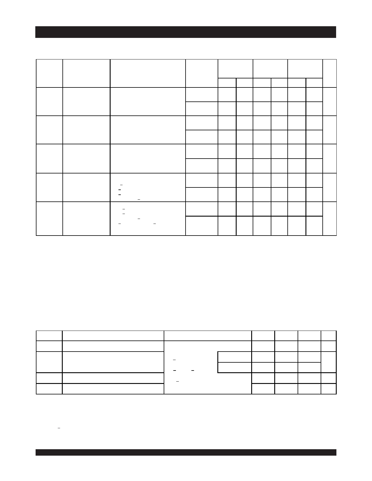
DC Electrical Characteristics Over the Operating
Temperature and Supply Voltage Range(1) (con’t.) (VCC = 5.0V ± 10%)
Symbol
Parameter
Test Condition
Version
7024X35
Com'l &
Military
Typ.(2) Max.
7024X55
Com'l, Ind
& Military
Typ.(2) Max.
7024X70
Military Only
Typ.(2) Max. Unit
ICC
Dynamic Operating
Current
(Both Ports Active)
CE = VIL,
Outputs Disabled
SEM = VIH
f = fMAX(3)
COM'L
MIL &
IND
S 150
250
150
250
____
L
150
210
150
210
____
____
mA
____
S 150 300 150 300 140 300
L 150 250 150 250 140 250
ISB1 Standby Current
(Both Ports - TTL
Level Inputs)
CER = CEL = VIH
SEMR = SEML = VIH
f = fMAX(3)
COM'L
S 13
60
13
60
____
____
mA
L 13
50
13
50
____
____
MIL &
IND
S 13
80
L 13
65
13
80
13
65
10
80
10
65
ISB2 Standby Current
(One Port - TTL
Level Inputs)
CE"A" = VIL and CE"B" = VIH(5)
Active Port Outputs Disabled,
f=fMAX(3)
SEMR = SEML = VIH
COM'L
S 85
155
95
155
____
____
mA
L 85
130
95
130
____
____
MIL &
IND
S 85
190
95
190
80
190
L
85
160
95
160
80
160
ISB3
Full Standby Current
Both Ports CEL and
(Both Ports -
CER > VCC - 0.2V,
CMOS Level Inputs)
VIN > VCC - 0.2V or
VIN < 0.2V, f = 0(4)
SEMR = SEML > VCC - 0.2V
ISB4 Full Standby Current
(One Port -
CMOS Level Inputs)
CE"A" < 0.2V and
CE"B" > VCC - 0.2V(5)
SEMR = SEML > VCC - 0.2V
VIN > VCC - 0.2V or VIN < 0.2V
Active Port Outputs Disabled,
f = fMAX(3)
COM'L
MIL &
IND
COM'L
MIL &
IND
S 1.0
15
1.0
15
____
____
mA
L 0.2
5
0.2
5
____
____
S 1.0
30
1.0
30
1.0
30
L 0.2
10
0.2
10
0.2
10
S 80
135
80
135
____
____
mA
L 80
110
80
110
____
____
S 80
175
80
175
75
175
L
80
150
80
150
75
150
NOTES:
2740 tbl 09b
1. 'X' in part number indicates power rating (S or L)
2. VCC = 5V, TA = +25°C, and are not production tested.
3. At f = fMAX, address and I/O'S are cycling at the maximum frequency read cycle of 1/tRC, and using “AC Test Conditions”of input levels of GND to 3V.
4. f = 0 means no address or control lines change.
5. Port "A" may be either left or right port. Port "B" is the opposite from port "A".
Data Retention Characteristics Over All Temperature Ranges
(L Version Only) (VLC = 0.2V, VHC = VCC - 0.2V)(4)
Symbol
Parameter
Test Condition
Min.
Typ.(1)
VDR
VCC for Data Retention
VCC = 2V
2.0
___
ICCDR
Data Retention Current
CE > VHC
MIL. & IND.
___
100
VIN > VHC or < VLC
COM'L.
___
100
tCDR(3)
Chip Deselect to Data Retention Time
SEM > VHC
0
___
tR(3)
Operation Recovery Time
tRC(2)
___
NOTES:
1. TA = +25°C, VCC = 2V, and are by device characterization but are not production tested.
2. tRC = Read Cycle Time
3. This parameter is guaranteed but not tested.
4. At Vcc < 2.0V, input leakages are not defined.
Max. Unit
___
V
4000 µ A
1500
___
ns
___
ns
2740 tbl 10
6.642
Share Link: 