570AILF データシートの表示(PDF) - Integrated Circuit Systems
部品番号
コンポーネント説明
一致するリスト
570AILF Datasheet PDF : 9 Pages
| |||
ICS570
Multiplier and Zero Delay Buffer
Description
The ICS570 is a high-performance Zero Delay Buffer
(ZDB) which integrates ICS’ proprietary analog/digital
Phase Locked Loop (PLL) techniques. The A version is
recommended for 5 V designs and the B version for
3.3 V designs. The chip is part of ICS’ ClockBlocksTM
family, and was designed as a performance upgrade to
meet today’s higher speed and lower voltage
requirements. The zero delay feature means that the
rising edge of the input clock aligns with the rising
edges of both output clocks, giving the appearance of
no delay through the device. There are two outputs on
the chip, one being a low-skew divide by two of the
other output. The device incorporates an all-chip power
down/tri-state mode that stops the internal PLL and
puts both outputs into a high impedance state.
The ICS570 is ideal for synchronizing outputs in a large
variety of systems, from personal computers to data
communications to graphics/video. By allowing off-chip
feedback paths, the device can eliminate the delay
through other devices.
The ICS570 A and B versions were designed to
improve input to output jitter from the original ICS570M
version, and are recommended for all new designs.
Features
• 8-pin SOIC package
• Available in Pb (lead) free package (A and B versions
only)
• Pin-for-pin replacement and upgrade to ICS570M
• Functional equivalent to AV9170 (not a pin-for-pin
replacement)
• Low input to output skew of 300 ps max (>60 MHz
outputs)
• Ability to choose between 14 different multipliers
from 0.5x to 32x
• Output clock frequency up to 168 MHz at 3.3 V
• Can recover degraded input clock duty cycle
• Output clock duty cycle of 45/55
• Power Down and Tri-State Mode
• Passes spread spectrum clock modulation
• Full CMOS clock swings with 25 mA drive capability
at TTL levels
• Advanced, low power CMOS process
• ICS570B has an operating voltage of 3.3 V (±5%)
• ICS570A has an operating voltage of 5.0 V (±5%)
• Industrial temperature version available
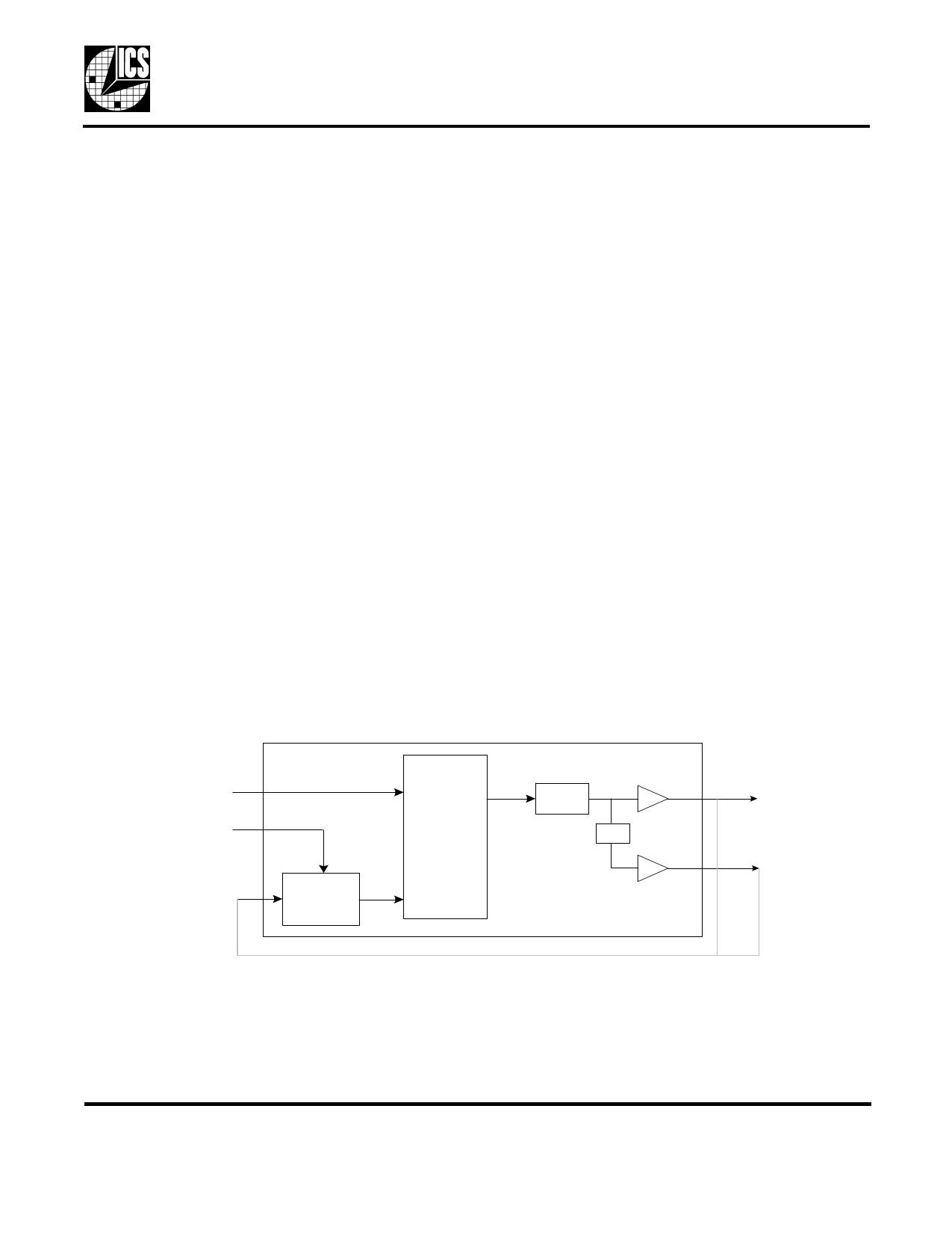
Block Diagram
IC L K
S 1 :0
F B IN
divide
by N
Phase
D e te c to r,
C ha rg e
Pum p,
and Loop
F ilte r
VCO
/2
CLK
CLK2
External feedback can com e from C LK or C LK/2 (see table on page 2)
MDS 570 I
1
Revision 030905
Integrated Circuit Systems, Inc. ● 525 Race Street, San Jose, CA 95126 ● tel (408) 297-1201 ● www.icst.com
Share Link: 