HSP3824 データシートの表示(PDF) - Harris Semiconductor
部品番号
コンポーネント説明
一致するリスト
HSP3824 Datasheet PDF : 41 Pages
| |||
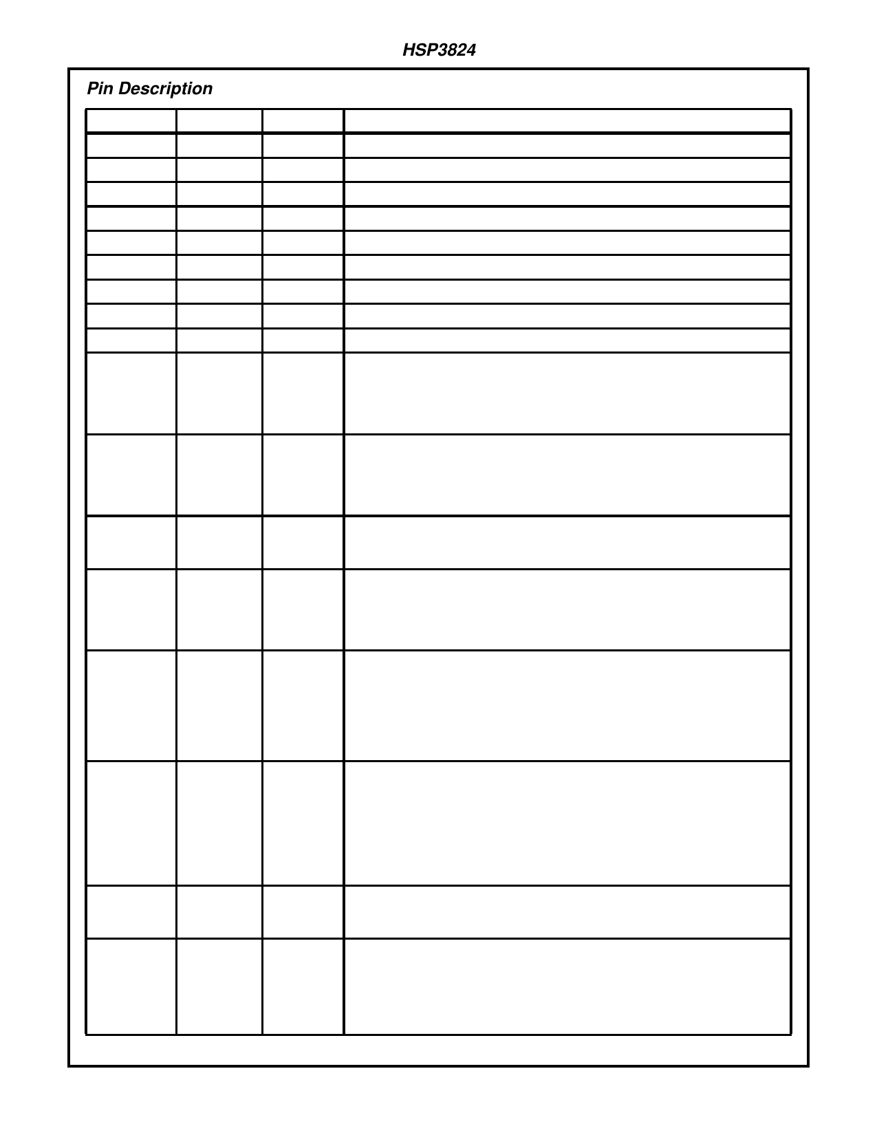
Pin Description
NAME
VDD (Analog)
VDD (Digital)
GND (Analog)
GND (Digital)
VREFN
VREFP
IIN
QIN
RSSI
A/D_CAL
PIN
10, 18, 20
7, 21, 29, 42
11, 15, 19
6, 22, 31, 41
17
16
12
13
14
26
TX_PE
2
TXD
3
TXCLK
4
TX_RDY
5
CCA
32
RXD
35
RXCLK
36
HSP3824
TYPE I/O
Power
Power
Ground
Ground
I
I
I
I
I
O
I
I
O
O
O
O
O
DESCRIPTION
DC power supply 2.7V - 5.5V
DC power supply 2.7V - 5.5V
DC power supply 2.7V - 5.5V, ground.
DC power supply 2.7V - 5.5V, ground.
“Negative” voltage reference for ADC’s (I and Q) [Relative to VREFP]
“Positive” voltage reference for ADC’s (I, Q and RSSI)
Analog input to the internal 3-bit A/D of the In-phase received data.
Analog input to the internal 3-bit A/D of the Quadrature received data.
Receive Signal Strength Indicator Analog input.
This signal is used internally as part of the I and Q ADC calibration circuit. When the
ADC calibration circuit is active, the voltage references of the ADCs are adjusted to
maintain the outputs of the ADCs in their optimum range. A logic 1 on this pin indicates
that one or both of the ADC outputs are at their full scale value. This signal can be
integrated externally as a control voltage for an external AGC.
When active, the transmitter is configured to be operational, otherwise the transmitter
is in standby mode. TX_PE is an input from the external Media Access Controller
(MAC) or network processor to the HSP3824. The rising edge of TX_PE will start the
internal transmit state machine and the falling edge will inhibit the state machine.
TX_PE envelopes the transmit data.
TXD is an input, used to transfer serial Data or Preamble/Header information bits from
the MAC or network processor to the HSP3824. The data is received serially with the
LSB first. The data is clocked in the HSP3824 at the falling edge of TXCLK.
TXCLK is a clock output used to receive the data on the TXD from the MAC or network
processor to the HSP3824, synchronously. Transmit data on the TXD bus is clocked
into the HSP3824 on the falling edge. The clocking edge is also programmable to be
on either phase of the clock. The rate of the clock will be depending upon the
modulation type and data rate that is programmed in the signalling field of the header.
When the HSP3824 is configured to generate the preamble and Header information
internally, TX_RDY is an output to the external network processor indicating that
Preamble and Header information has been generated and that the HSP3824 is ready
to receive the data packet from the network processor over the TXD serial bus. The
TX_RDY returns to the inactive state when the TX_PE goes inactive indicating the end
of the data transmission. TX_RDY is an active high signal. This signal is meaningful
only when the HSP3824 generates its own preamble.
Clear Channel Assessment (CCA) is an output used to signal that the channel is clear
to transmit. The CCA algorithm is user programmable and makes its decision as a
function of RSSI, Energy detect (ED), Carrier Sense (CRS) and the CCA watch dog
timer. The CCA algorithm and its programmable features are described in the data
sheet.
Logic 0 = Channel is clear to transmit.
Logic 1 = Channel is NOT clear to transmit (busy).
NOTE: This polarity is programmable and can be inverted.
RXD is an output to the external network processor transferring demodulated Header
information and data in a serial format. The data is sent serially with the LSB first. The
data is frame aligned with MD_RDY.
RXCLK is the clock output bit clock. This clock is used to transfer Header information
and data through the RXD serial bus to the network processor. This clock reflects the
bit rate in use.RXCLK will be held to a logic “0” state during the acquisition process.
RXCLK becomes active when the HSP3824 enters in the data mode. This occurs once
bit sync is declared and a valid signal quality estimate is made, when comparing the
programmed signal quality thresholds.
4
Share Link: 