EL7560 データシートの表示(PDF) - Intersil
部品番号
コンポーネント説明
一致するリスト
EL7560 Datasheet PDF : 7 Pages
| |||
EL7560
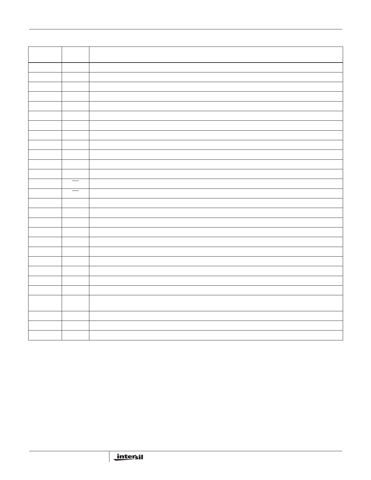
EL7560 Pin Descriptions
PIN
NUMBER
1
2
3
4
5
6
7
8
9
10
11
12
13
14
NAME
DESCRIPTION
CP- Negative input for the charge pump bootstrap capacitor. (Note 1)
CP+ Positive input for the charge pump bootstrap capacitor. (Note 1)
C2V Voltage doubler output. Pin requires at least a 1µF capacitor to GND. (Note 1)
VSS Ground return for the control circuitry.
VHI Positive supply for the high side driver. This pin is bootstrapped from the LX pin with a 0.1µF capacitor.
LX Common connection between the two large internal FETs. External inductor connection.
LX Same as pin 6.
LX Same as pin 6.
LX Same as pin 6.
LX Same as pin 6.
TEST This is test pin and must remain grounded at all times
PWRGD Pin pulls high when the FB pin is within - 7%(typ) of its programmed value.
OT Overtemperature indicator. Pulls low when the die temperature exceeds 135°C. Pin has 10mA pull-up.
OT A logic high on OUTEN enables the regulator (Note 1)
15
VID3 Bit 3(MSB) of the output voltage select DAC.
16
VID2 Bit 2 of the output voltage select DAC.
17
VID1 Bit 1 of the output voltage select DAC.
18
VID0 Bit 0(LSB) of the output voltage select DAC.
19
VSSP Ground return to the buck regulator.
20
VSSP Same as pin 19.
21
VIN Positive power supply input to the buck regulator.
22
VSSP Same as pin 19.
23
VIN Same as pin 21.
24
VDD Pin supplies power to the internal control circuitry.
25
COSC Oscillator timing capacitor. Oscillator Frequency is approximately: FOSC(Hz)=0.0001/COSC(F). The duty cycle is
approximately 5%. (Note 1)
26
CSLOPE Slope compensation capacitor.
27
CREF External reference input pin.
28
FB Voltage feedback pin for the buck regulator.
NOTE:
1. The oscillator and voltage doubler operate normally when VDD exceeds VDD-ON threshold, independent of the OUTEN logic level.
4
Share Link: 