DS21348 データシートの表示(PDF) - Dallas Semiconductor -> Maxim Integrated
部品番号
コンポーネント説明
一致するリスト
DS21348 Datasheet PDF : 73 Pages
| |||
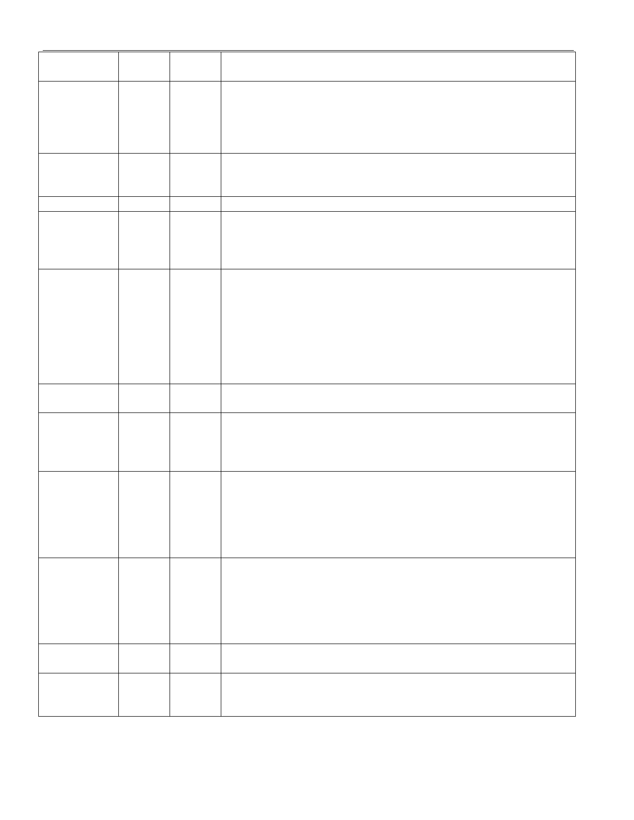
ACRONYM PIN
MCLK
30
MM0/
18/
MM1
19
NA
-
NRZE
3
PBEO
24
RCLK
40
RCL
25
RNEG
39
RPOS
38
RT0/
44/
RT1
23
RTIP/
27/
RRING
28
I/O DESCRIPTION
DS21348/Q348
I Master Clock. A 2.048MHz (±50ppm) clock source with TTL
levels is applied at this pin. This clock is used internally for both
clock/data recovery and for jitter attenuation. Use of a T1 1.544MHz
clock source is optional.
See Note 2.
I Monitor Mode Select Bits 0 & 1 [H/W Mode]. These inputs
determine if the receive equalizer is in a monitor mode.
See Table 4-8.
I Not Assigned. Should be tied low.
I NRZ Enable [H/W Mode].
0 = Bipolar data at RPOS/RNEG and TPOS/TNEG
1 = NRZ data at RPOS and TPOS or TNEG; RNEG outputs a
positive going pulse when device receives a BPV, CV, or EXZ.
O PRBS Bit Error Output. The receiver will constantly search for a
215-1 or a 220-1 PRBS depending on the ETS bit setting (CCR1.7).
Remains high if out of synchronization with the PRBS pattern.
Goes low when synchronized to the PRBS pattern. Any errors in the
received pattern after synchronization will cause a positive going
pulse (with same period as E1 or T1 clock) synchronous with
RCLK. PRBS bit errors can also be reported to the ECR1 and
ECR2 registers by setting CCR6.2 to a logic 1.
O Receive Clock. Buffered recovered clock from the line.
Synchronous to MCLK in absence of signal at RTIP and RRING.
O Receive Carrier Loss. An output which will toggle high during a
receive carrier loss (CCR2.7 = 0) or will toggle high if the TCLK
pin has not been toggled for 5 msec ± 2 msec (CCR2.7 = 1). CCR2.7
defaults to logic 0 when in hardware mode.
O Receive Negative Data. Updated on the rising edge (CCR2.0 = 0)
or the falling edge (CCR2.0 = 1) of RCLK with the bipolar data out
of the line interface. Set NRZE (CCR1.6) to a one for NRZ
applications. In NRZ mode, data will be output on RPOS while a
received error will cause a positive-going pulse synchronous with
RCLK at RNEG. See section 8.4 for details.
O Receive Positive Data. Updated on the rising edge (CCR2.0 = 0) or
the falling edge (CCR2.0 = 1) of RCLK with bipolar data out of the
line interface. Set NRZE (CCR1.6) to a one for NRZ applications.
In NRZ mode, data will be output on RPOS while a received error
will cause a positive-going pulse synchronous with RCLK at RNEG.
See section 8.4 for details.
I Receive LIU Termination Select Bits 0 & 1 [H/W Mode]. These
inputs determine the receive termination. See Table 4-9.
I Receive Tip and Ring. Analog inputs for clock recovery circuitry.
These pins connect via a 1:1 transformer to the line. See Section 7
for details.
18 of 73
Share Link: 