CY7C1339B-166 データシートの表示(PDF) - Cypress Semiconductor
部品番号
コンポーネント説明
一致するリスト
CY7C1339B-166 Datasheet PDF : 17 Pages
| |||
CY7C1339B
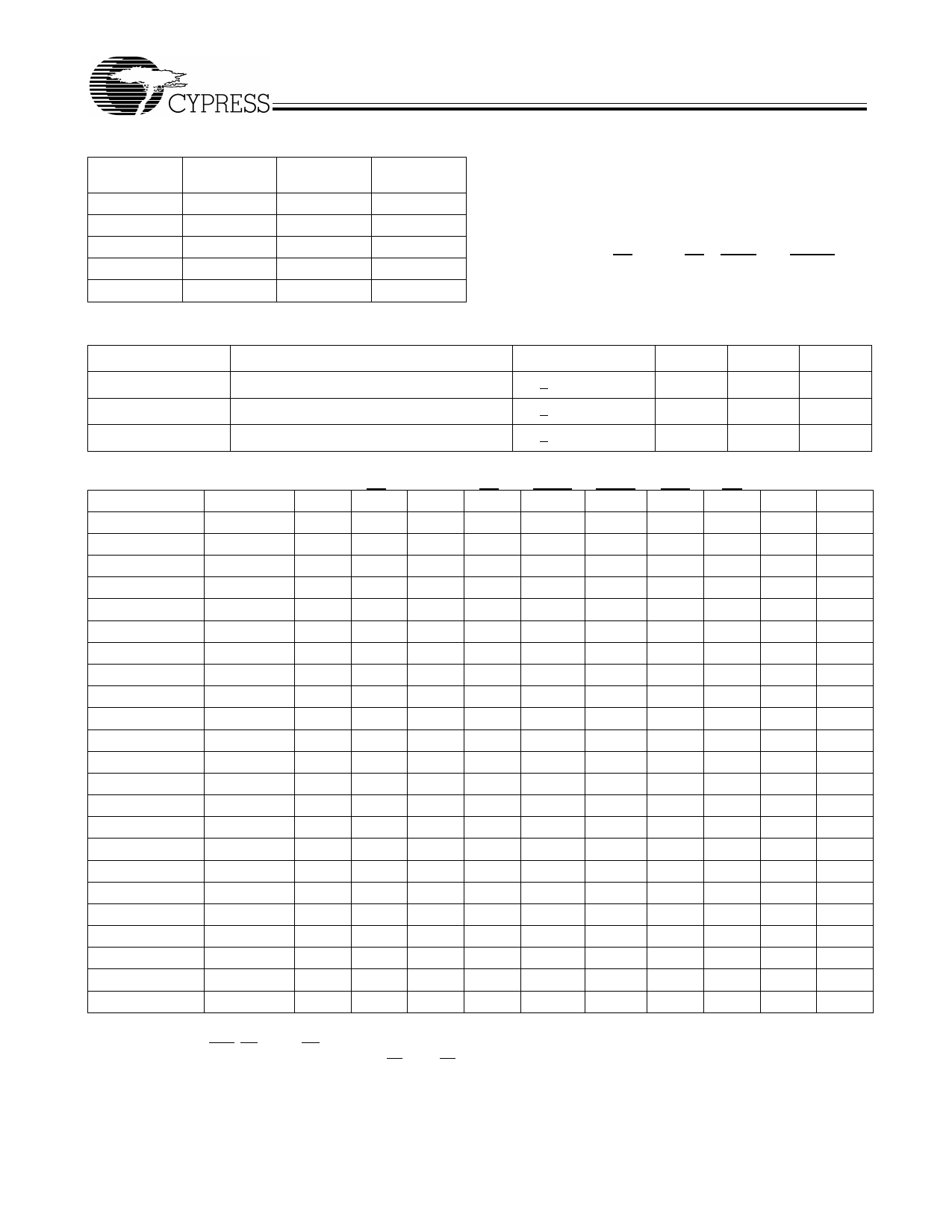
Linear Burst Sequence
First
Address
A[1:0]
00
01
10
11
Second
Address
A[1:0]
01
10
11
00
Third
Address
A[1:0]
10
11
00
01
Fourth
Address
A[1:0]
11
00
01
10
Sleep Mode
The ZZ input pin is an asynchronous input. Asserting ZZ
places the SRAM in a power conservation “sleep” mode. Two
clock cycles are required to enter into or exit from this “sleep”
mode. While in this mode, data integrity is guaranteed.
Accesses pending when entering the “sleep” mode are not
considered valid nor is the completion of the operation
guaranteed. The device must be deselected prior to entering
the “sleep” mode. CE1, CE2, CE3, ADSP, and ADSC must
remain inactive for the duration of tZZREC after the ZZ input
returns LOW.
ZZ Mode Electrical Characteristics
Parameter
IDDZZ
tZZS
tZZREC
Description
Snooze mode standby current
Device operation to ZZ
ZZ recovery time
Test Conditions
ZZ > VDD – 0.2V
ZZ > VDD – 0.2V
ZZ < 0.2V
Min.
2tCYC
Max.
3
2tCYC
Unit
mA
ns
ns
Cycle Descriptions[1, 2, 3]
Next Cycle Add. Used ZZ
Unselected
None
L
CE3 CE2 CE1 ADSP ADSC ADV OE
DQ Write
X
X
1
X
0
X
X Hi-Z X
Unselected
None
L
1
X
0
0
X
X
X Hi-Z X
Unselected
None
L
X
0
0
0
X
X
X Hi-Z X
Unselected
None
L
1
X
0
1
0
X
X Hi-Z X
Unselected
None
L
X
0
0
1
0
X
X Hi-Z X
Begin Read
External
L
0
1
0
0
X
X
X Hi-Z X
Begin Read
External
L
0
1
0
1
0
X
X Hi-Z Read
Continue Read Next
L
X
X
X
1
1
0
1 Hi-Z Read
Continue Read Next
L
X
X
X
1
1
0
0 DQ Read
Continue Read Next
L
X
X
1
X
1
0
1 Hi-Z Read
Continue Read Next
L
X
X
1
X
1
0
0 DQ Read
Suspend Read Current
L
X
X
X
1
1
1
1 Hi-Z Read
Suspend Read Current
L
X
X
X
1
1
1
0 DQ Read
Suspend Read Current
L
X
X
1
X
1
1
1 Hi-Z Read
Suspend Read Current
L
X
X
1
X
1
1
0 DQ Read
Begin Write
Current
L
X
X
X
1
1
1
X Hi-Z Write
Begin Write
Current
L
X
X
1
X
1
1
X Hi-Z Write
Begin Write
External
L
0
1
0
1
0
X
X Hi-Z Write
Continue Write Next
L
X
X
X
1
1
0
X Hi-Z Write
Continue Write Next
L
X
X
1
X
1
0
X Hi-Z Write
Suspend Write Current
L
X
X
X
1
1
1
X Hi-Z Write
Suspend Write Current
L
X
X
1
X
1
1
X Hi-Z Write
ZZ “Sleep”
None
H
X
X
X
X
X
X
X Hi-Z X
Notes:
1. X = “Don't Care,” 1 = HIGH, 0 = LOW.
2. Write is defined by BWE, BW[3:0], and GW. See Write Cycle Descriptions table.
3. The DQ pins are controlled by the current cycle and the OE signal. OE is asynchronous and is not sampled with the clock.
Document #: 38-05141 Rev. *A
Page 6 of 17
Share Link: 