PDI1394P11 データシートの表示(PDF) - Philips Electronics
部品番号
コンポーネント説明
一致するリスト
PDI1394P11 Datasheet PDF : 20 Pages
| |||
Philips Semiconductors
3-port physical layer interface
Product specification
PDI1394P11
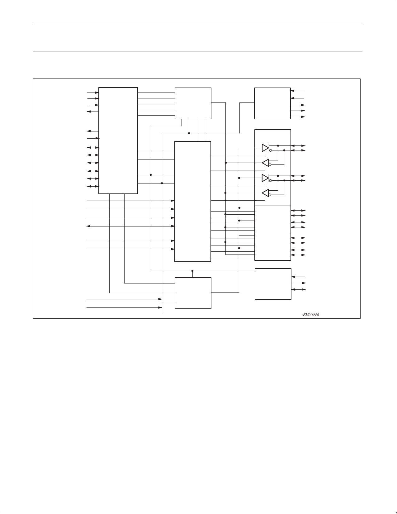
6.0 BLOCK DIAGRAM
CPS
LPS
ISO–
CNA
SYSCLK
LREQ
CTL0
CTL1
D0
D1
D2
D3
PC0
PC1
PC2
C/LKON
TESTM1
TESTM2
LINK
INTERFACE
RECEIVED
DATA
DECODER/
TIMER
ARBITRATION
AND CONTROL
STATE
MACHINE
LOGIC
BIAS
VOLTAGE AND
CURRENT
GENERATOR
PORT 1
R0
R1
TPBIAS1
TPBIAS2
TPBIAS3
TPA1+
TPA1–
TPB1+
TPB1–
PORT 2
PORT 3
TPA2+
TPA2–
TPB2+
TPB2–
TPA3+
TPA3–
TPB3+
TPB3–
RESET–
PD
TRANSMIT
DATA
ENCODER
CRYSTAL
OSCILLATOR
PLL SYSTEM
& TRANSMIT
CLOCK
GENERATOR
XI
XO
FILTER
SV00228
7.0 FUNCTIONAL SPECIFICATION
The PDI1394P11 is an IEEE1394–1995 High Performance Serial
Bus Specification compliant physical layer interface device. It
provides an interface between an attached link layer controller and
three 1394 cable interface ports. In addition to the interface function,
the PDI1394P11 performs bus initialization and arbitration functions
as well as monitoring line conditions and connection status.
7.1 Clocking
The PDI1394P11 utilizes a stable internal reference clock of
196.608 MHz. The reference clock is generated using an external
24.576 MHz crystal and an internal Phase Locked Loop (PLL). The
PLL clock is divided down to 49.152 MHz and 98.304 MHz clock
signals. The 49.152 MHz clock is used for internal logic and
provided as an output to clock a link layer controller. The 196.608
MHz and 98.304 MHz clocks are used for synchronization of the
transmitted strobe and data information.
7.2 Port Interfaces
The PDI1394P11 provides the transceiver functions needed to
implement a three port node in a cable-based 1394 network. Each
cable port incorporates two differential line transceivers. In addition
to transmission and reception of packet data, the line transceivers
monitor conditions on the cable to determine connection status, data
speed, and bus arbitration states.
The PDI1394P11 receives data to be transmitted over the bus from
two or four parallel data paths to the Link Controller, D[0:3]. These
data paths are latched and synchronized with the 49.152 MHz clock.
The parallel bit paths are combined serially, encoded and
transmitted at either 98.304 Mb/s or 196.608 Mb/s, depending
whether the transaction is a 100 Mb/s or 200 Mb/s transfer,
respectively. The transmitted data is encoded as data-strobe
information, with the data information being transmitted on the TPB
cable pairs and the strobe information transmitted on the TPA cable
pairs.
During packet reception the TPA and TPB transmitters of the
receiving cable port are disabled, and the receivers for that port are
enabled. The encoded data information is received on the TPA cable
pair and the strobe information is received on the TPB cable pair.
The combination of the data and strobe signals is decoded to
recover the receive clock signal and the serial data stream. The
serial data stream is converted to two or four parallel bit streams,
resynchronized to the internal 49.152 MHz clock and sent to the
1999 Apr 09
4
Share Link: 