AT-38086 データシートの表示(PDF) - HP => Agilent Technologies
部品番号
コンポーネント説明
一致するリスト
AT-38086 Datasheet PDF : 10 Pages
| |||
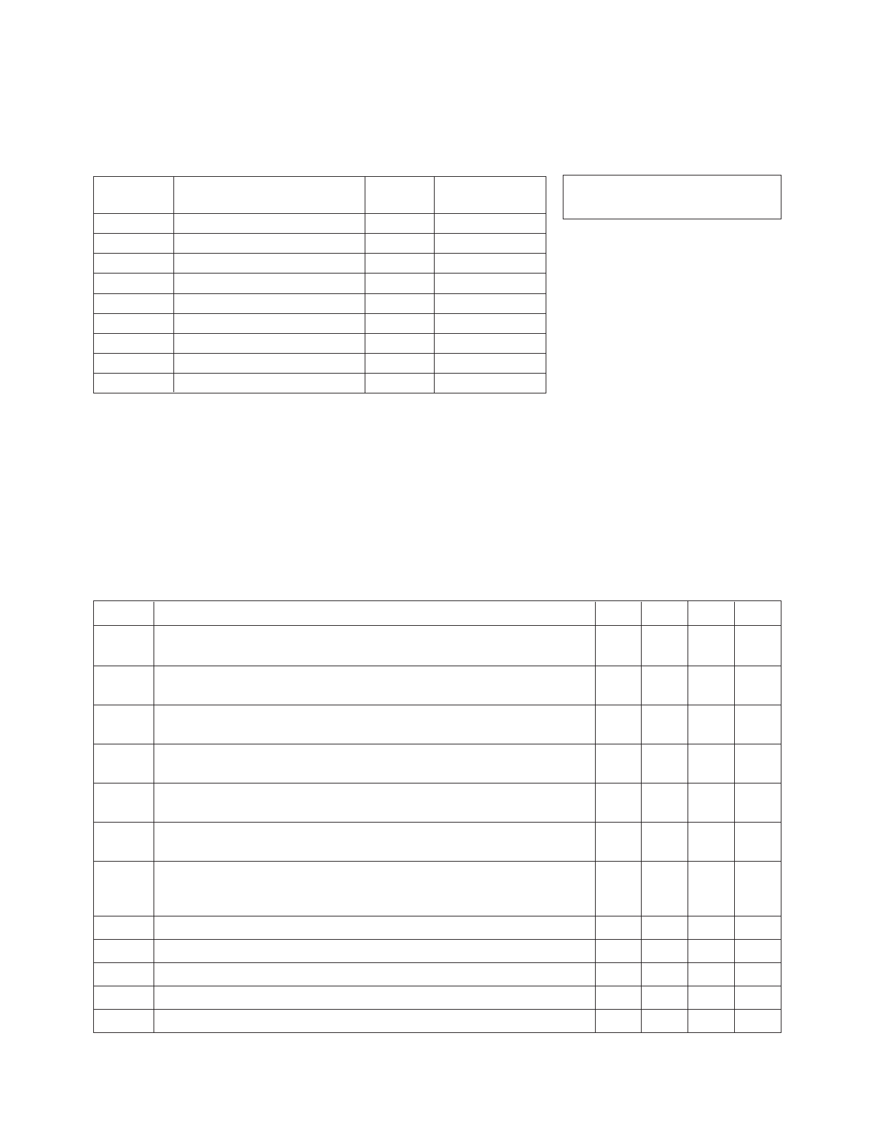
AT-38086 Absolute Maximum Ratings
Symbol
Parameter
Units
Absolute
Maximum[1]
VEBO
Emitter-Base Voltage
V
1.4
VCBO
Collector-Base Voltage
V
16.0
VCEO
Collector-Emitter Voltage
V
9.5
IC
Collector Current[2]
mA
250
IC
Collector Current[3]
mA
160
PT
Peak Power Dissipation [2, 4] W
3.7
PT
CW Power Dissipation [3, 5] mW
460
Tj
Junction Temperature
°C
150
TSTG
Storage Temperature
°C
-65 to 150
Notes:
1. Permanent damage may occur if any of these limits are exceeded.
2. Pulsed operation, pulse width = 577␣ µsec, duty cycle␣ =␣ 12.5%.
3. CW operation.
4. Derate at 57.1 mW/°C for TC␣ >␣ 85 °C. TC is defined to be the temperature of the
collector pin 3, where the lead contacts the circuit board.
5. Derate at 7.1 mW/°C for TC␣ >␣ 85 °C. TC is defined to be the temperature of the
collector pin 3, where the lead contacts the circuit board.
6. Using the liquid crystal technique, VCE = 4.5 V, Ic = 50 mA, Tj =150°C, 1-2␣ µm
“hot-spot” resolution.
Thermal Resistance[6]:
θjc = 140°C/W
Electrical Specifications, TC = 25°C
Symbol
Parameters and Test Conditions
Units Min. Typ. Max.
Freq. = 900 MHz, VCE = 4.8 V, ICQ = 20 mA, Pulse width = 577 µsec,
duty cycle = 12.5%, unless otherwise specified
Pout
Output Power,
Pulsed Operation[1]
Test Circuit A, Pin = +17 dBm dBm +26.5 +28.0
ηC
Collector Efficiency,
Pulsed Operation[1]
Test Circuit A, Pin = +17 dBm %
50
60
Mismatch Tolerance
Test Circuit A, Pout = +28 dBm,
7:1
No Damage, Pulsed[1]
any phase, 2 sec duration
Pout
Output Power,
CW Operation[2]
F = 836.5 MHz, ICQ = 15 mA dBm +22.0 +23.5
Test Circuit B, Pin = +10 dBm
IMD3 3rd Order Intermodulation Distortion,
F1 = 899 MHz, F2 = 901 MHz dBc
-35
2-Tone Test, Pout each tone = +17 dBm, CW[2,3] ICQ = 15 mA, Test Circuit B
Mismatch Tolerance, No Damage,
F = 836.5 MHz, ICQ = 15 mA
7:1
CW[2]
Test Circuit B, Pout = +23.5 dBm
any phase, 2 sec duration
BVEBO
BVCBO
BVCEO
hFE
ICEO
Emitter-Base Breakdown Voltage
Collector-Base Breakdown Voltage
Collector-Emitter Breakdown Voltage
Forward Current Transfer Ratio
Collector Leakage Current
IE = 0.2 mA, open collector V
1.4
IC = 1.0 mA, open emitter V 16.0
IC = 3.0 mA, open base V
9.5
VCE = 3 V, IC = 160 mA —
40
150 330
VCEO = 5 V µA
15
Notes:
1. With external matching on input and output, tested in a 50 ohm environment. Refer to Test Circuit A (GSM).
2. With external matching on input and output, tested in a 50 ohm environment. Refer to Test Circuit B (AMPS).
3. Test circuit B re-tuned at 900␣ MHz.
4-90
Share Link: 