AIC1620 データシートの表示(PDF) - Analog Intergrations
部品番号
コンポーネント説明
一致するリスト
AIC1620 Datasheet PDF : 12 Pages
| |||
AIC1620/AIC1621/AIC1622
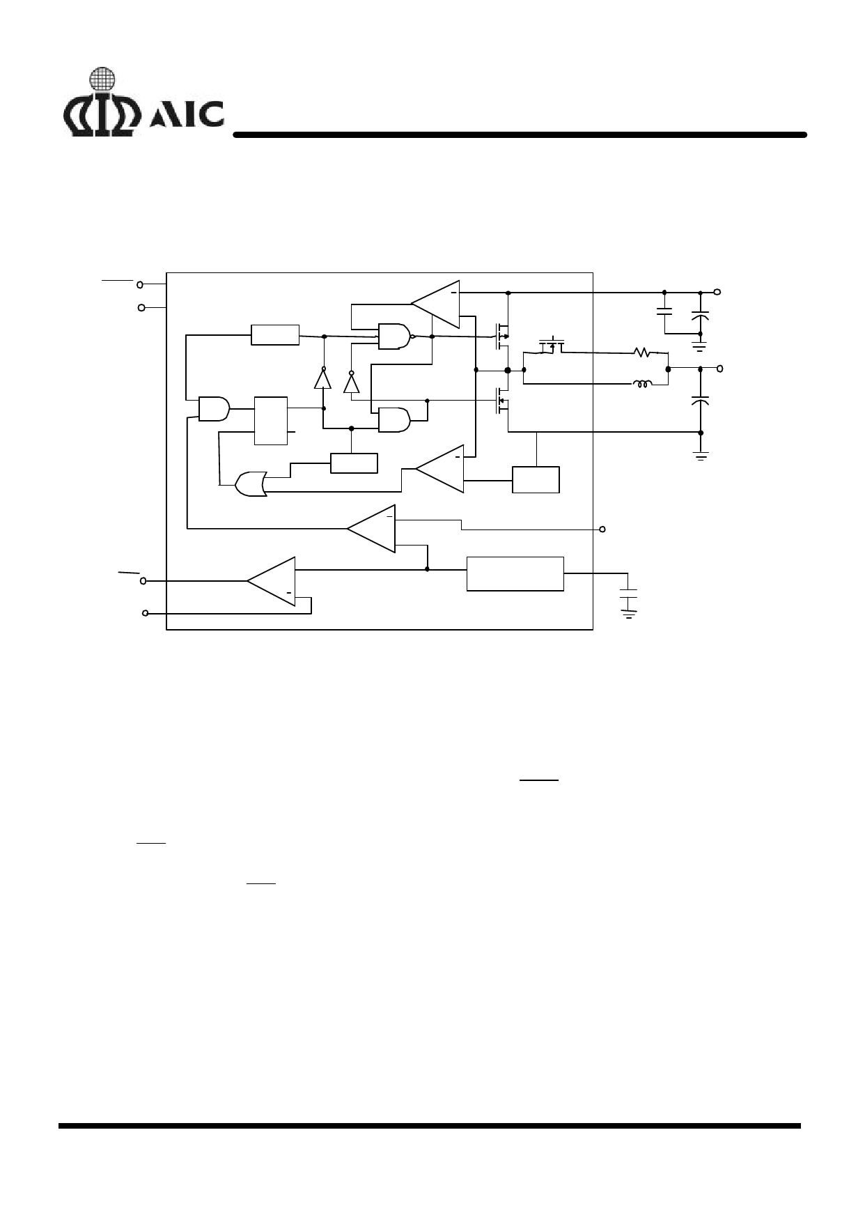
n BLOCK DIAGRAM
SHDN
CLSEL
LBO
LBI
Minimum Off-Time
One Shot
F/F
SQ
R
One Shot
Maximum On-Time
+
+
OUT
+
Q1
Damping
0.1µF
Switch
R1
Q3
BATT 200Ω
Q2
LX
L
1
4 7µF
GND
+
Mirror
OUT
C3
220µF
VIN
+ C1
100µF
Reference Voltage
FB
REF
C4
0.1µF
n PIN DESCRIPTIONS
AIC1620/ AIC1621
PIN 1: FB- Connect to OUT for +3.3V output.
Use a resistor network to set the
output voltage from +1.8V to +4.0V.
PIN 2: LBI- Low-battery comparator input. nI ter-
nally set to trip at +1.23V.
PIN 3: LBO- Open-drain low battery comparator
output. Output is low when VLBI is
<1.23V. LBO is high impedance
during shutdown.
PIN 4: REF- 1.23V reference voltage. Bypass
with a 0.1µF capacitor.
PIN 5: SHDN- Shutdown input. High=operating,
low=shutdown.
PIN 6: GND- Ground
PIN 7: LX- N-channel and P-channel power
MOSFET drain.
PIN 8: OUT- Power output. OUT provides boot-
strap power to the IC.
7
Share Link: 