AIC1620 データシートの表示(PDF) - Analog Intergrations
部品番号
コンポーネント説明
一致するリスト
AIC1620 Datasheet PDF : 12 Pages
| |||
AIC1620/AIC1621/AIC1622
Component Selection
1. Inductor Selection
An inductor value of 22µH performs well in most
applications. The AIC1620 series also work with
inductors in the 10µH to 47µH range. An inductor
with higher peak inductor current tends a higher
output voltage ripple (IPEAK×output filter capacitor
ESR). The inductor’s DC resistance significantly
affects efficiency. We can calculate the maximum
output current as follows:
IOUT (MAX)
=
VIN
VOUT
ILIM
−
t OFF
VOUT − VIN
2×L
η
where IOUT(MAX)=maximum output current in
amps
VIN=input voltage
L=inductor value in µH
η=efficiency (typically 0.9)
tOFF=LX switch’off-time in µS
ILIM=0.45A or 0.8A
2. Capacitor Selection
The output voltage ripple relates with the peak in-
ductor current and the output capacitor ESR. Be-
sides output ripple voltage, the output ripple cur-
rent also needs to be concerned. The smaller the
capacitor ESR is, the higher the ripple current will
be. A filter capacitor with low ESR is helpful to
the efficiency and steady state output current of
AIC1620 series. Therefore HERMEI capacitor LT
series with 220µF/6.3V is recommended. A
smaller capacitor (down to 10F with higher ESR)
is acceptable for light loads or in applications that
can tolerate higher output ripple.
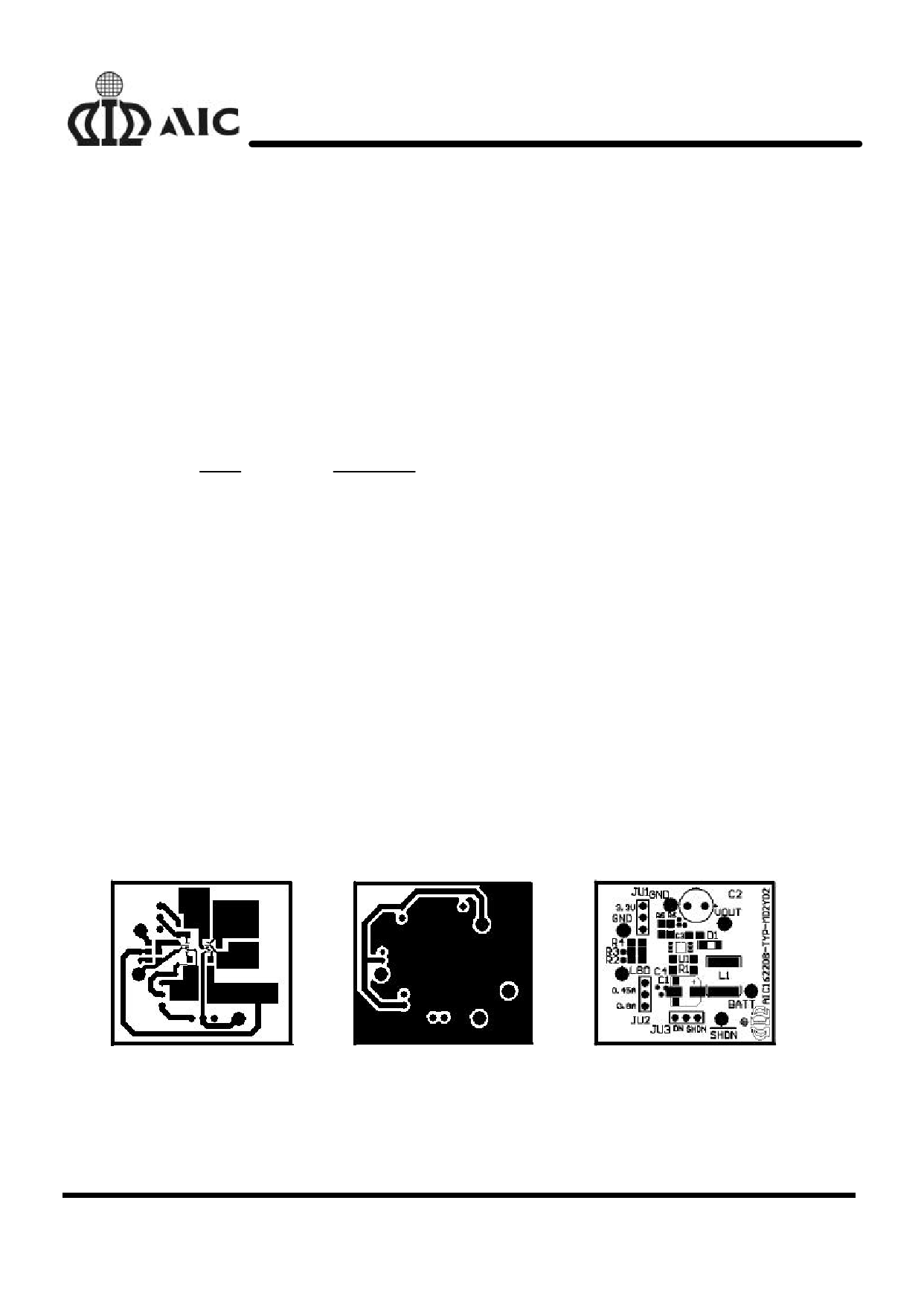
3. PCB Layout and Grounding
Since AIC1622’s switching frequency can range
up to 500kHz, it makes AIC1622 become very
sensitive. So careful printed circuit layout is mi -
portant for minimizing ground bounce and noise.
IC’s OUT pin should be as clear as possible. And
the GND pin should be placed close to the ground
plane. Keep the IC’s GND pin and the ground
leads of the input and output filter capacitors less
than 0.2in (5mm) apart. In addition, keep all con-
nection to the FB and LX pins as short as possi-
ble. In particular, when using external feedback
resistors, locate them as close to the FB as pos-
sible. To maximize output power and efficiency
and minimize output ripple voltage, use a ground
plane and solder the IC’s GND directly to the
ground plane. Following are the recommended
layout diagrams.
Figure 12. Top layer
Figure 13. Bottom layer
Figure 14. Placement
10
Share Link: 