ADN4665 データシートの表示(PDF) - Analog Devices
部品番号
コンポーネント説明
一致するリスト
ADN4665 Datasheet PDF : 12 Pages
| |||
THEORY OF OPERATION
The ADN4665 is a quad line driver for low voltage differential
signaling. It takes a single-ended 3 V logic signal and converts
it to a differential current output. The data can then be trans-
mitted for considerable distances, over media such as a twisted pair
cable or PCB backplane, to an LVDS receiver such as the ADN4666,
where it develops a voltage across a termination resistor, RT. This
resistor is chosen to match the characteristic impedance of the
medium, typically around 100 Ω. The differential voltage is
detected by the receiver and converted back into a single-ended
logic signal.
When DINx is high (Logic 1), current flows out of the DOUTx+
pin (current source) through RT and back into the DOUTx− pin
(current sink). At the receiver, this current develops a positive
differential voltage across RT (with respect to the inverting input)
and results in a Logic 1 at the receiver output. When DINx is low,
DOUTx+ sinks current and DOUTx− sources current; a negative dif-
ferential voltage across RT results in a Logic 0 at the receiver output.
The output drive current is between ±2.5 mA and ±4.5 mA
(typically ±3.5 mA), developing between ±250 mV and ±450 mV
across a 100 Ω termination resistor. The received voltage is centered
around the receiver offset of 1.25 V. Therefore, the noninverting
receiver input is typically 1.375 V (that is, 1.2 V + [350 mV/2]) and
the inverting receiver input is 1.025 V (that is, 1.2 V − [350 mV/2])
for Logic 1. For Logic 0, the inverting and noninverting output
voltages are reversed. Note that because the differential voltage
reverses polarity, the peak-to-peak voltage swing across RT is
twice the differential voltage.
Current-mode drivers offer considerable advantages over voltage-
mode drivers such as RS-422 drivers. The operating current
remains fairly constant with increased switching frequency,
whereas the operating current of voltage-mode drivers increases
exponentially in most cases. This is caused by the overlap current as
internal gates switch between high and low, which causes currents
to flow from the device power supply to ground. A current-mode
device simply reverses a constant current between its two outputs,
with no significant overlap currents.
ADN4665
This is similar to emitter-coupled logic (ECL) and positive
emitter-coupled logic (PECL), but without the high quiescent
current of ECL and PECL.
ENABLE INPUTS
The active high and active low enable inputs deactivate all the
current drivers when the drivers are in the disabled state. This
also powers down the device and reduces the current consumption
from typically 23 mA to typically 2.6 mA. A truth table for the
enable inputs is shown in Table 5.
Table 5. Enable Inputs Truth Table
Pin Logic Level
EN
EN
DINx
Low
High
X1
Low
Low
Low
Low
Low
High
High
Low
Low
High
Low
High
DOUTx+
Inactive
ISINK
ISOURCE
ISINK
ISOURCE
DOUTx−
Inactive
ISOURCE
ISINK
ISOURCE
ISINK
1 X = don’t care.
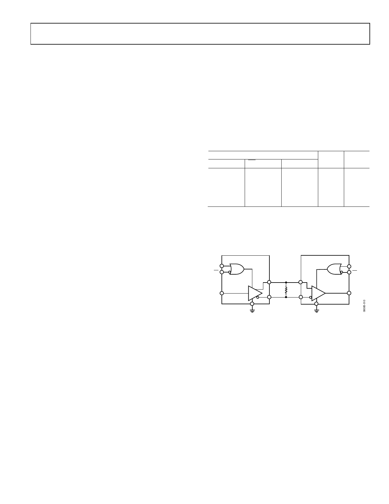
APPLICATIONS INFORMATION
Figure 10 shows a typical application for point-to-point data
transmission using the ADN4665 as the driver.
1/4 ADN4665
EN
EN
DINx
GND
RECEIVER
DOUTx+ RINy+
RT
100Ω
DOUTx– RINy–
GND
EN
EN
ROUTy
Figure 10. Typical Application Circuit
Rev. 0 | Page 9 of 12
Share Link: 