AD8346 データシートの表示(PDF) - Analog Devices
部品番号
コンポーネント説明
一致するリスト
AD8346 Datasheet PDF : 20 Pages
| |||
AD8346
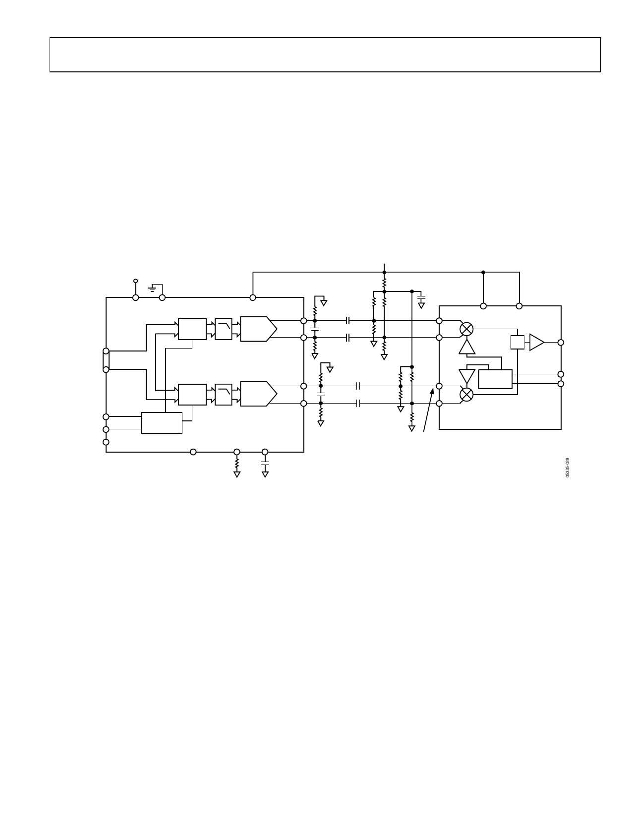
AC-COUPLED INTERFACE
An ac-coupled interface can also be implemented, as shown in
Figure 29. This is an advantage because there is almost no
voltage loss due to the biasing network, allowing the AD8346
inputs to be driven by the full 2 V p-p differential signal from
the AD9761 (each of the DAC’s 4 outputs delivering 1 V p-p).
As in the dc-coupled case, the bias levels on the I and Q inputs
should be set to as precise a level as possible, relative to each
other. This prevents the introduction of additional input offset
voltages. In Figure 29, the bias level on each input is set to
approximately 1.2 V. The 2.43 kΩ resistors should have a ratio
tolerance of 0.1% or better.
5V
DVDD DCOM
LATCH
I
2×
AVDD
I
DAC
IOUTA
IOUTB
DAC
DATA
INPUTS
SELECT
WRITE
LATCH
Q
MUX
CONTROL
CLOCK
SLEEP
AD9761
QOUTA
Q
2×
DAC
QOUTB
FS ADJ REFIO
RSET
2kΩ
0.1μF
The network shown has a high-pass corner frequency of
approximately 14.3 kHz (note that the 12 kΩ input impedance
of the AD8346 has been factored into this calculation).
Increasing the resistors in the network or increasing the
coupling capacitance reduces the corner frequency further.
Note that the LO suppression can be manually optimized by
replacing a portion of the four top 2.43 kΩ resistors with
potentiometers. In this case, the bottom four resistors in the
biasing network no longer need to be precision devices.
5V
2.43kΩ
100Ω 0.01μF
CFILTER 2.43kΩ
100Ω 0.01μF
1kΩ
2.43kΩ
2.43kΩ
0.1μF
IBBP
VPS1
IBBN
VPS2
VOUT
Σ
100Ω 0.01μF 2.43kΩ
2.43kΩ
QBBP
CFILTER
2.43kΩ
100Ω 0.01μF
2.43kΩ
QBBN
1V p-p EACH PIN
WITH VCM = 1.2V
PHASE
SPLITTER
AD8346
LOIP
LOIN
Figure 29. AC-Coupled DAC Interface
Rev. A | Page 13 of 20
Share Link: 