MC100EL34DR2(2000) データシートの表示(PDF) - ON Semiconductor
部品番号
コンポーネント説明
一致するリスト
MC100EL34DR2 Datasheet PDF : 8 Pages
| |||
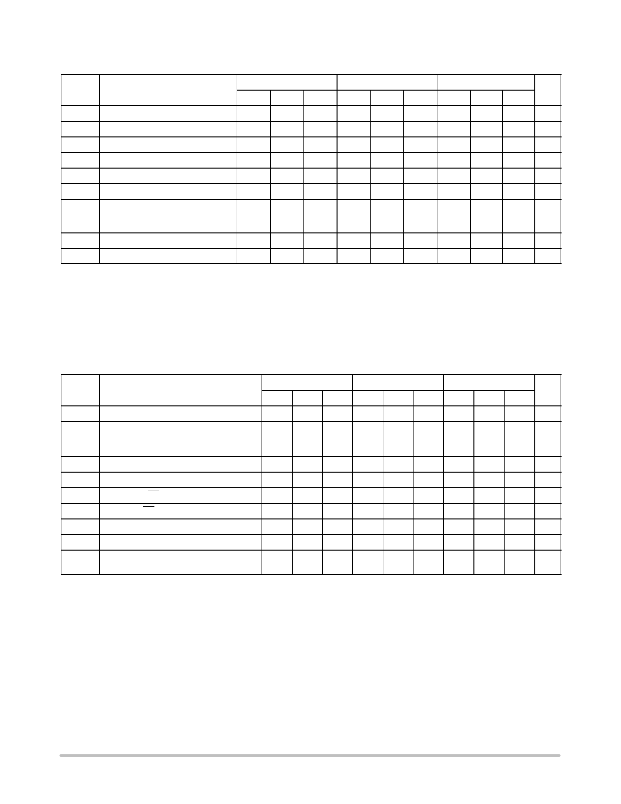
MC10EL34, MC100EL34
AC CHARACTERISTICS VCC= 5.0 V; VEE= 0.0 V or VCC= 0.0 V; VEE= –5.0 V (Note 1.)
–40°C
25°C
Symbol
Characteristic
Min Typ Max Min Typ Max Min
fmax
Maximum Toggle Frequency
TBD
TBD
tPLH
Propagation
tPHL
Delay to
Output
CLK to Q0
960
CLK to Q1,2
900
MR to Q
750
1200 960
1140 900
1060 750
1200 970
1140 910
1060 790
tSKEW
Within-Device Skew (Note 2.)
100
100
tJITTER
Cycle–to–Cycle Jitter
TBD
TBD
tS
Setup Time EN
400
400
400
tH
Hold Time EN
250
250
250
tRR
Set/Reset Recovery
400 200
400 200
400
VPP
Input Swing (Note 3.)
150
1000 150
1000 150
tr
Output Rise/Fall Times Q
tf
(20% – 80%)
275
525 275
525 275
1. 10 Series: VEE can vary +0.06 V / –0.5 V.
100 Series: VEE can vary +0.8 V / –0.5 V.
2. Within-device skew is defined as identical transitions on similar paths through a device.
3. VPP(min) is minimum input swing for which AC parameters guaranteed. The device has a DC gain of ≈40.
85°C
Typ Max
TBD
1210
1150
1090
100
TBD
200
1000
525
Unit
GHz
ps
ps
ps
ps
ps
ps
mV
ps
tRR
RESET
Internal Clock
Disabled
Internal Clock
Enabled
CLK
Q0
Q1
Q2
EN
The EN signal will freeze the internal clocks to the flip–flops on the first falling edge of CLK after its assertion. The internal
dividers will maintain their state during the internal clock freeze and will return to clocking once the internal clocks are unfrozen.
The outputs will transition to their next states in the same manner, time and relationship as they would have had the EN signal
not been asserted.
Figure 1. Timing Diagram
http://onsemi.com
5
Share Link: 