MC10EL34D(2000) データシートの表示(PDF) - ON Semiconductor
部品番号
コンポーネント説明
一致するリスト
MC10EL34D Datasheet PDF : 8 Pages
| |||
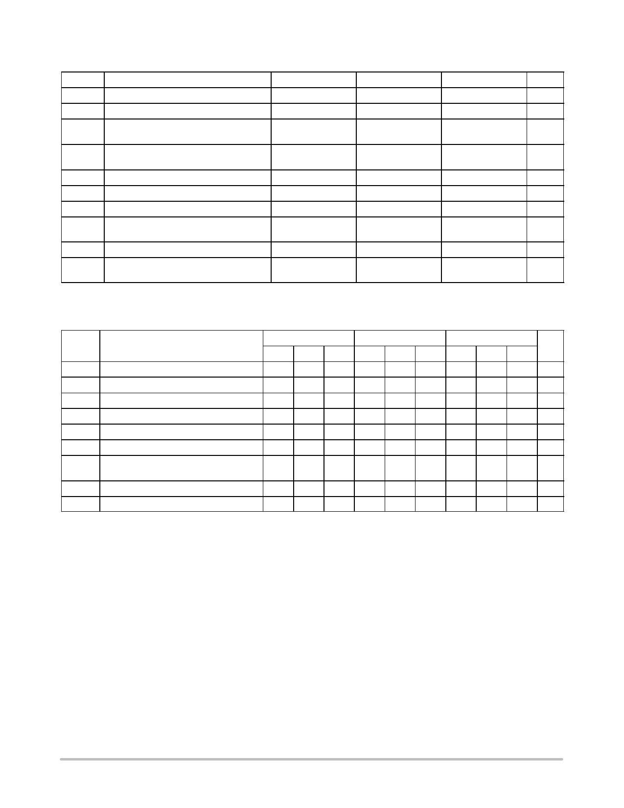
MC10EL34, MC100EL34
10EL SERIES PECL DC CHARACTERISTICS VCC= 5.0 V; VEE= 0.0 V (Note 1.)
–40°C
25°C
85°C
Symbol
Characteristic
Min Typ Max Min Typ Max Min Typ Max Unit
IEE
VOH
VOL
VIH
VIL
VBB
VIHCMR
Power Supply Current
Output HIGH Voltage (Note 2.)
Output LOW Voltage (Note 2.)
Input HIGH Voltage (Single Ended)
Input LOW Voltage (Single Ended)
Output Voltage Reference
Input HIGH Voltage Common Mode
Range (Differential) (Note 3.)
39
39
39 mA
3920 4010 4110 4020 4105 4190 4090 4185 4280 mV
3050 3200 3350 3050 3210 3370 3050 3227 3405 mV
3770
4110 3870
4190 3940
4280 mV
3050
3500 3050
3520 3050
3555 mV
3.57
3.7 3.65
3.75 3.69
3.81 V
3.0
4.6 3.0
4.6 3.0
4.6
V
IIH
Input HIGH Current
150
150
150 µA
IIL
Input LOW Current
0.5
0.5
0.3
µA
NOTE: Devices are designed to meet the DC specifications shown in the above table, after thermal equilibrium has been established. The
circuit is in a test socket or mounted on a printed circuit board and transverse air flow greater than 500 lfpm is maintained.
1. Input and output parameters vary 1:1 with VCC. VEE can vary +0.06 V / –0.5 V.
2. Outputs are terminated through a 50 ohm resistor to VCC–2 volts.
3. VIHCMR min varies 1:1 with VEE, VIHCMR max varies 1:1 with VCC. The VIHCMR range is referenced to the most positive side of the differential input
signal. Normal operation is obtained if the HIGH level falls within the specified range and the peak-to-peak voltage lies between VPPmin and 1V.
10EL SERIES NECL DC CHARACTERISTICS VCC= 0.0 V; VEE= –5.0 V (Note 1.)
–40°C
25°C
85°C
Symbol
Characteristic
Min Typ Max Min Typ Max Min Typ Max Unit
IEE
VOH
VOL
VIH
VIL
VBB
VIHCMR
Power Supply Current
Output HIGH Voltage (Note 2.)
Output LOW Voltage (Note 2.)
Input HIGH Voltage (Single Ended)
Input LOW Voltage (Single Ended)
Output Voltage Reference
Input HIGH Voltage Common Mode
Range (Differential) (Note 3.)
39
39
39 mA
–1080 –990 –890 –980 –895 –810 –910 –815 –720 mV
–1950 –1800 –1650 –1950 –1790 –1630 –1950 –1773 –1595 mV
–1230
–890 –1130
–810 –1060
–720 mV
–1950
–1500 –1950
–1480 –1950
–1445 mV
–1.43
–1.30 –1.35
–1.25 –1.31
–1.19 V
–2.0
–0.4 –2.0
–0.4 –2.0
–0.4 V
IIH
Input HIGH Current
150
150
150 µA
IIL
Input LOW Current
0.5
0.5
0.3
µA
NOTE: Devices are designed to meet the DC specifications shown in the above table, after thermal equilibrium has been established. The
circuit is in a test socket or mounted on a printed circuit board and transverse air flow greater than 500 lfpm is maintained.
1. Input and output parameters vary 1:1 with VCC. VEE can vary +0.06 V / –0.5 V.
2. Outputs are terminated through a 50 ohm resistor to VCC–2 volts.
3. VIHCMR min varies 1:1 with VEE, VIHCMR max varies 1:1 with VCC. The VIHCMR range is referenced to the most positive side of the differential input
signal. Normal operation is obtained if the HIGH level falls within the specified range and the peak-to-peak voltage lies between VPPmin and 1V.
http://onsemi.com
3
Share Link: 