R5F2127 データシートの表示(PDF) - Renesas Electronics
部品番号
コンポーネント説明
一致するリスト
R5F2127 Datasheet PDF : 75 Pages
| |||
R8C/26 Group, R8C/27 Group
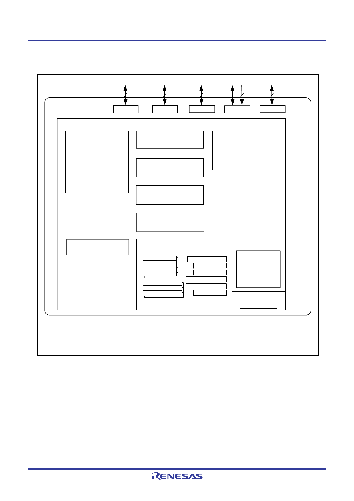
1.3 Block Diagram
Figure 1.1 shows a Block Diagram.
1. Overview
8
8
6
13
2
I/O ports
Port P0
Port P1
Port P3
Port P4
Port P5
Peripheral functions
Timers
Timer RA (8 bits)
Timer RB (8 bits)
Timer RC
(16 bits × 1 channel)
Timer RE (8 bits)
A/D converter
(10 bits × 12 channels)
UART or
clock synchronous serial I/O
(8 bits × 2 channels)
I2C bus interface or clock synchronous
serial I/O with chip select
(8 bits × 1 channel)
System clock
generation circuit
XIN-XOUT
High-speed on-chip oscillator
Low-Speed on-chip oscillator
XCIN-XCOUT(3)
LIN module
(1 channel)
Watchdog timer
(15 bits)
R8C CPU core
R0H R0L
R1H R1L
R2
R3
A0
A1
FB
SB
USP
ISP
INTB
PC
FLG
Memory
ROM(1)
RAM(2)
Multiplier
Figure 1.1 Block Diagram
NOTES:
1. ROM size varies with MCU type.
2. RAM size varies with MCU type.
3. XCIN, XCOUT can be used only for N or D version.
Rev.2.10 Sep 26, 2008 Page 4 of 69
REJ03B0168-0210
Share Link: 