R5F2127 データシートの表示(PDF) - Renesas Electronics
部品番号
コンポーネント説明
一致するリスト
R5F2127 Datasheet PDF : 75 Pages
| |||
R8C/26 Group, R8C/27 Group
1. Overview
1.2 Performance Overview
Table 1.1 outlines the Functions and Specifications for R8C/26 Group and Table 1.2 outlines the Functions and
Specifications for R8C/27 Group.
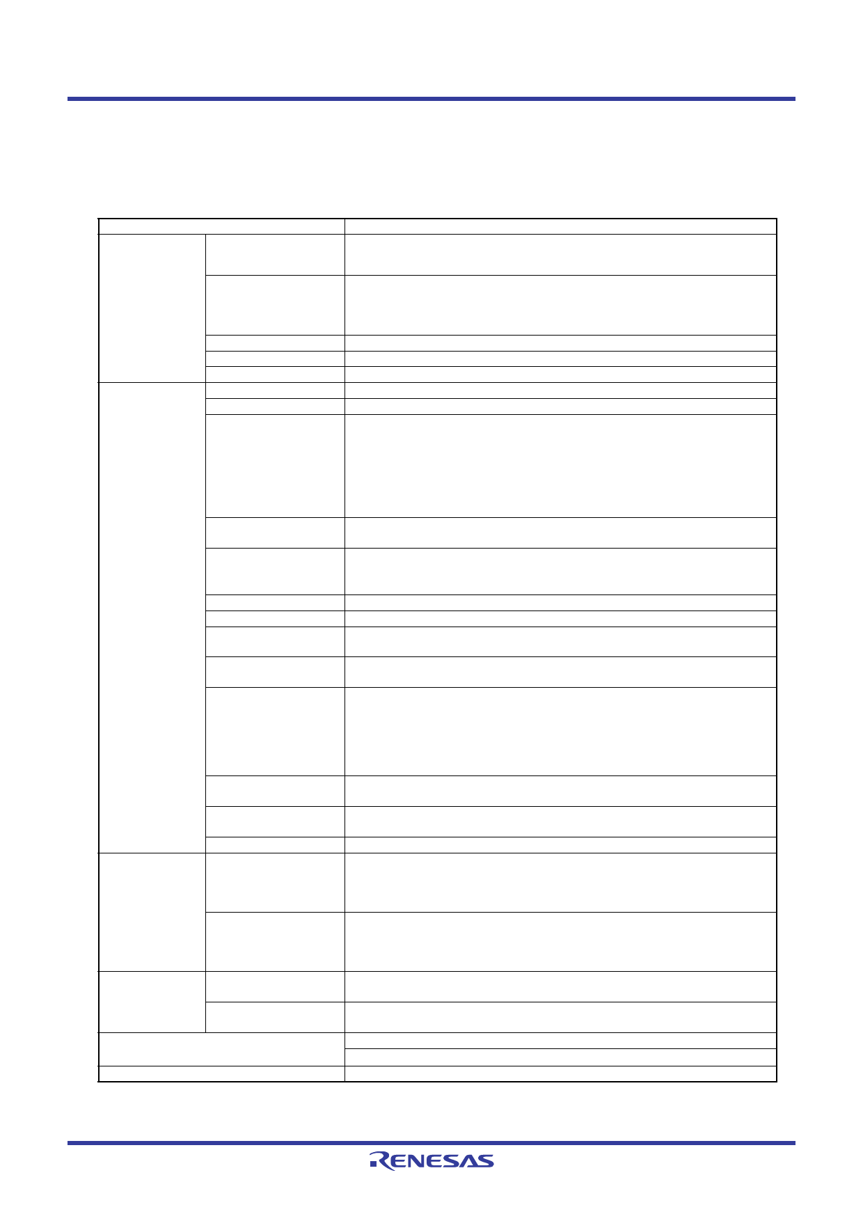
Table 1.1 Functions and Specifications for R8C/26 Group
CPU
Peripheral
Functions
Item
Number of
fundamental
instructions
Minimum instruction
execution time
Operating mode
Address space
Memory capacity
Ports
LED drive ports
Timers
Serial interfaces
Clock synchronous
serial interface
LIN module
A/D converter
Watchdog timer
Interrupts
Clock generation
circuits
Electrical
Characteristics
Oscillation-stopped
detector
Voltage detection
circuit
Power-on reset circuit
Supply voltage
Current consumption
(N, D version)
Flash Memory Programming and
erasure voltage
Programming and
erasure endurance
Operating Ambient Temperature
Package
89 instructions
Specification
50 ns (f(XIN) = 20 MHz, VCC = 3.0 to 5.5 V) (other than K version)
62.5 ns (f(XIN) = 16 MHz, VCC = 3.0 to 5.5 V) (K version)
100 ns (f(XIN) = 10 MHz, VCC = 2.7 to 5.5 V)
200 ns (f(XIN) = 5 MHz, VCC = 2.2 to 5.5 V) (N, D version)
Single-chip
1 Mbyte
Refer to Table 1.3 Product Information for R8C/26 Group
I/O ports: 25 pins, Input port: 3 pins
I/O ports: 8 pins (N, D version)
Timer RA: 8 bits × 1 channel
Timer RB: 8 bits × 1 channel
(Each timer equipped with 8-bit prescaler)
Timer RC: 16 bits × 1 channel
(Input capture and output compare circuits)
Timer RE: With real-time clock and compare match function
(For J, K version, compare match function only.)
2 channels (UART0, UART1)
Clock synchronous serial I/O, UART
1 channel
I2C bus Interface(1)
Clock synchronous serial I/O with chip select
Hardware LIN: 1 channel (timer RA, UART0)
10-bit A/D converter: 1 circuit, 12 channels
15 bits × 1 channel (with prescaler)
Start-on-reset selectable
Internal: 15 sources, External: 4 sources,
Software: 4 sources, Priority levels: 7 levels
3 circuits
• XIN clock generation circuit (with on-chip feedback resistor)
• On-chip oscillator (high speed, low speed)
High-speed on-chip oscillator has a frequency adjustment function
• XCIN clock generation circuit (32 kHz) (N, D version)
• Real-time clock (timer RE) (N, D version)
XIN clock oscillation stop detection function
On-chip
On-chip
VCC = 3.0 to 5.5 V (f(XIN) = 20 MHz) (other than K version)
VCC = 3.0 to 5.5 V (f(XIN) = 16 MHz) (K version)
VCC = 2.7 to 5.5 V (f(XIN) = 10 MHz)
VCC = 2.2 to 5.5 V (f(XIN) = 5 MHz) (N, D version)
Typ. 10 mA (VCC = 5.0 V, f(XIN) = 20 MHz)
Typ. 6 mA (VCC = 3.0 V, f(XIN) = 10 MHz)
Typ. 2.0 µA (VCC = 3.0 V, wait mode (f(XCIN) = 32 kHz)
Typ. 0.7 µA (VCC = 3.0 V, stop mode)
VCC = 2.7 to 5.5 V
100 times
-20 to 85°C (N version)
-40 to 85°C (D, J version)(2), -40 to 125°C (K version)(2)
32-pin molded-plastic LQFP
NOTES:
1. I2C bus is a trademark of Koninklijke Philips Electronics N. V.
2. Specify the D, K version if D, K version functions are to be used.
Rev.2.10 Sep 26, 2008 Page 2 of 69
REJ03B0168-0210
Share Link: 