MAX3421E データシートの表示(PDF) - Maxim Integrated
部品番号
コンポーネント説明
一致するリスト
MAX3421E Datasheet PDF : 28 Pages
| |||
MAX3421E
USB Peripheral/Host Controller
with SPI Interface
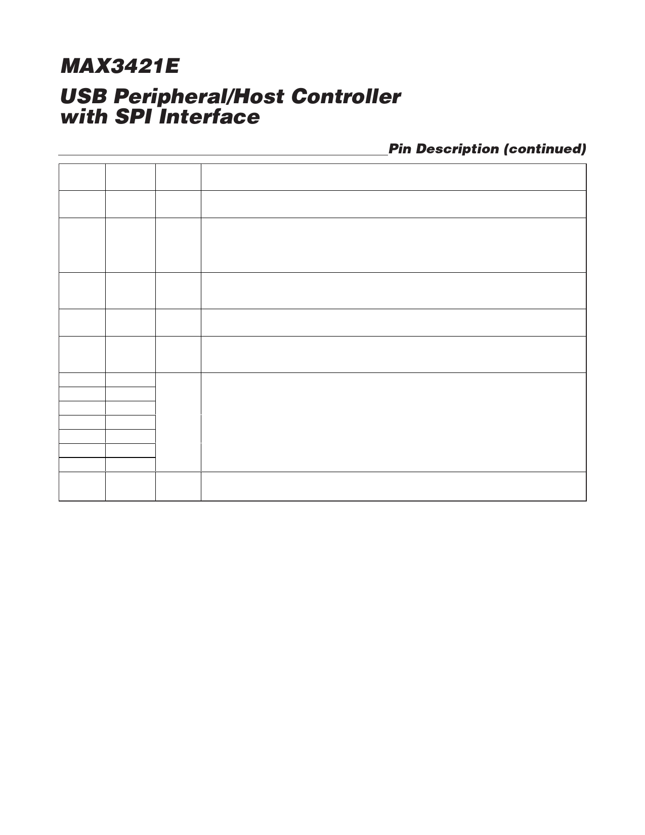
Pin Description (continued)
PIN
NAME
INPUT/
OUTPUT
FUNCTION
21
D+
Input/ USB D+ Signal. Connect D+ to a USB connector through a 33Ω ±1% series resistor. A
Output switchable 1.5kΩ D+ pullup resistor and 15kΩ D+ pulldown resistor is internal to the device.
VBUS Comparator Input. VBCOMP is internally connected to a voltage comparator to allow the
SPI master to detect (through an interrupt or checking a register bit) the presence or loss of
22
VBCOMP
Input power on VBUS. Bypass VBCOMP to ground with a 1.0µF ceramic capacitor. VBCOMP is pulled
down to ground with RIN (see Electrical Characteristics).
23
VCC
Input
USB Transceiver and Logic Core Power-Supply Input. Connect VCC to a positive 3.3V power
supply. Bypass VCC to ground with a 1.0µF ceramic capacitor as close to the VCC pin as possible.
Crystal Oscillator Input. Connect XI to one side of a parallel resonant 12MHz ±0.25% crystal
24
XI
Input and a load capacitor to GND. XI can also be driven by an external clock referenced to VCC.
25
XO
Output
Crystal Oscillator Output. Connect XO to the other side of a parallel resonant 12MHz ±0.25% crystal
and a load capacitor to GND. Leave XO unconnected if XI is driven with an external source.
26
GPIN0
27
GPIN1
28
GPIN2
29
GPIN3
Input
General-Purpose Inputs. GPIN7–GPIN0 are connected to VL with internal pullup resistors.
GPIN7–GPIN0 logic levels are referenced to the voltage on VL.
30
GPIN4
31
GPIN5
32
GPIN6
—
EP
Input
Exposed Pad, Connected to Ground. Connect EP to GND or leave unconnected. EP is located on
the bottom of the TQFN package. The TQFP package does not have an exposed pad.
6
Maxim Integrated
Share Link: 