MAX3421E データシートの表示(PDF) - Maxim Integrated
部品番号
コンポーネント説明
一致するリスト
MAX3421E Datasheet PDF : 28 Pages
| |||
MAX3421E
USB Peripheral/Host Controller
with SPI Interface
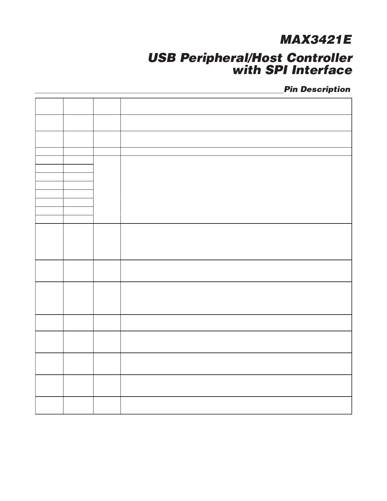
PIN
1
2
3, 19
4
5
6
7
8
9
10
11
12
13
14
15
16
17
18
20
Pin Description
NAME
GPIN7
VL
GND
GPOUT0
GPOUT1
GPOUT2
GPOUT3
GPOUT4
GPOUT5
GPOUT6
GPOUT7
RES
SCLK
SS
INPUT/
OUTPUT
FUNCTION
Input General-Purpose Input. GPIN7–GPIN0 are connected to VL with internal pullup resistors.
GPIN7–GPIN0 logic levels are referenced to the voltage on VL.
Input
Input
Level-Translator Voltage Input. Connect VL to the system’s 1.4V to 3.6V logic-level power
supply. Bypass VL to ground with a 0.1µF capacitor as close to VL as possible.
Ground
Output
General-Purpose Push-Pull Outputs. GPOUT7–GPOUT0 logic levels are referenced to the
voltage on VL.
Input
Input
Input
Device Reset. Drive RES low to clear all of the internal registers except for PINCTL (R17),
USBCTL (R15), and SPI logic. The logic level is referenced to the voltage on VL. (See the
Device Reset section for a description of resets available on the MAX3421E.) Note: The
MAX3421E is internally reset if either VCC or VL is not present. The register file is not accessible
under these conditions.
SPI Serial-Clock Input. An external SPI master supplies SCLK with frequencies up to 26MHz. The
logic level is referenced to the voltage on VL. Data is clocked into the SPI slave interface on the
rising edge of SCLK. Data is clocked out of the SPI slave interface on the falling edge of SCLK.
SPI Slave Select Input. The SS logic level is referenced to the voltage on VL. When SS is driven
high, the SPI slave interface is not selected, the MISO pin is high impedance, and SCLK
transitions are ignored. An SPI transfer begins with a high-to-low SS transition and ends with a
low-to-high SS transition.
MISO
MOSI
GPX
INT
D-
Output
Input or
Input/
Output
Output
Output
Input/
Output
SPI Serial-Data Output (Master-In Slave-Out). MISO is a push-pull output. MISO is tri-stated in
half-duplex mode or when SS = 1. The MISO logic level is referenced to the voltage on VL.
SPI Serial-Data Input (Master-Out Slave-In). The logic level on MOSI is referenced to the
voltage on VL. MOSI can also be configured as a bidirectional MOSI/MISO input and output.
(See Figure 15.)
General-Purpose Multiplexed Push-Pull Output. The internal MAX3421E signal that appears on
GPX is programmable by writing to the GPXB and GPXA bits of the PINCTL (R17) register and the
SEPIRQ bit of the MODE (R27) register. GPX indicates one of five signals (see the GPX section).
Interrupt Output. In edge mode, the logic level on INT is referenced to the voltage on VL and is
a push-pull output with programmable polarity. In level mode, INT is open-drain and active low.
Set the IE bit in the CPUCTL (R16) register to enable INT.
USB D- Signal. Connect D- to a USB connector through a 33Ω ±1% series resistor. A
switchable 15kΩ D- pulldown resistor is internal to the device.
Maxim Integrated
5
Share Link: 