MAX5391 データシートの表示(PDF) - Maxim Integrated
部品番号
コンポーネント説明
一致するリスト
MAX5391 Datasheet PDF : 14 Pages
| |||
MAX5391/MAX5393
Dual 256-Tap, Volatile, Low-Voltage
Linear Taper Digital Potentiometers
Detailed Description
The MAX5391/MAX5393 dual 256-tap, volatile, low-
voltage linear taper digital potentiometers offer three end-
toend resistance values of 10kΩ, 50kΩ, and 100kΩ. Each
potentiometer consists of 255 fixed resistors in series
between terminals H_ and L_. The potentiometer wiper,
W_, is programmable to access any one of the 256 tap
points on the resistor string.
The potentiometers in each device are programmable
independently of each other. The MAX5391/MAX5393
feature an SPI interface.
Charge Pump
The MAX5391/MAX5393 contain an internal charge pump
that guarantees the maximum wiper resistance, RWL, to
be less then 200Ω for supply voltages down to 1.7V. Pins
H_, W_, and L_ are still required to be less than VDD +
0.3V. A bypass input, BYP, is provided to allow additional
filtering of the charge-pump output, further reducing clock
feed through that may occur on H_, W_, or L_. The nomi-
nal clock rate of the charge pump is 600kHz. BYP should
remain resistively unloaded as any additional load would
produce a ripple of approximately IBYP/(600kHz x CBYP)
volts. See the Charge-Pump Feedthrough at W_ vs.
CBYP graph in the Typical Operating Characteristics for
CBYP sizing guidelines with respect to clock feedthrough
to the wiper. The value of CBYP does affect the startup
time of the charge pump; however, CBYP does not impact
the ability to communicate with the device, nor is there a
minimum CBYP requirement. The maximum wiper imped-
ance specification is not guaranteed until the charge
pump is fully settled. See the BYP Ramp vs. CBYP graph
in the Typical Operating Characteristics for CBYP impact
on charge-pump settling time.
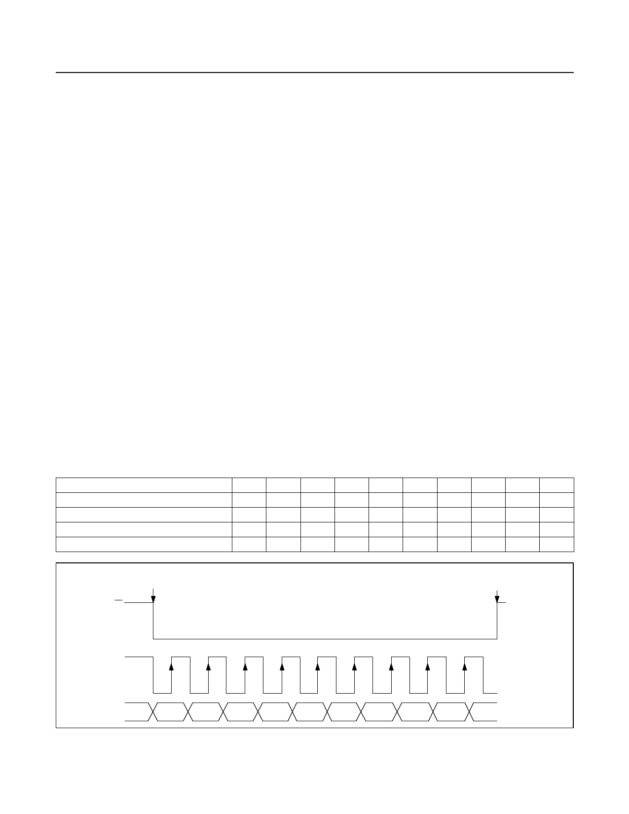
SPI Digital Interface
The MAX5391/MAX5393 include a SPI interface that pro-
vides a 3-wire write-only serial-data interface to control
the wiper tap position through inputs chip select (CS),
data in (DIN), and data clock (SCLK). Drive CS low to load
data from DIN synchronously into the serial shift register
on the rising edge of each SCLK pulse. The MAX5391/
MAX5393 load the last 10 bits of clocked data into the
appropriate potentiometer control register once CS transi-
tions high. See Figures 2 and 3. Data written to a memory
register immediately updates the wiper position. Keep CS
low during the entire data stream to prevent the data from
being terminated.
The first two bits A1:A0 (address bits) address one of
the two potentiometers. See Table 1. The power-on reset
(POR) circuitry sets the wiper to midscale.
Table 1. SPI Register Map
Bit Number
Bit Name
Write Wiper Register A
Write Wiper Register B
Write to Both A and B
1
2
3
4
5
6
7
8
9
10
A1
A0
D7
D6
D5
D4
D3
D2
D1
D0
0
0
D7
D6
D5
D4
D3
D2
D1
D0
0
1
D7
D6
D5
D4
D3
D2
D1
D0
1
1
D7
D6
D5
D4
D3
D2
D1
D0
COMMAND
STARTED 10-BIT
CS
WIPER REGISTER
LOADED
SCLK
DIN
A0
A1
D7
D6
D5
D4
D3
D2
D1
D0
Figure 2. SPI Digital Interface Format
www.maximintegrated.com
Maxim Integrated │ 9
Share Link: 