MAX5391 データシートの表示(PDF) - Maxim Integrated
部品番号
コンポーネント説明
一致するリスト
MAX5391 Datasheet PDF : 14 Pages
| |||
MAX5391/MAX5393
Dual 256-Tap, Volatile, Low-Voltage
Linear Taper Digital Potentiometers
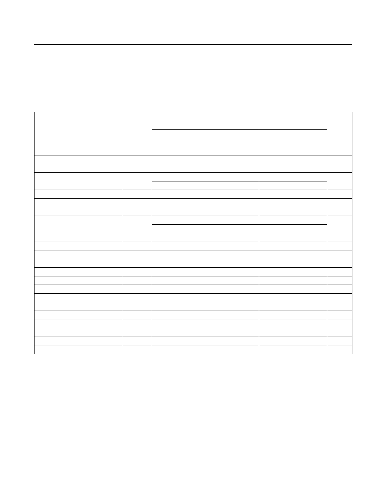
Electrical Characteristics (continued)
(VDD = +1.7V to +5.5V, VH_ = VDD, VL_ = 0V, TA = TMIN to TMAX, unless otherwise noted. Typical values are at VDD = +1.8V,
TA = +25°C.) (Note 1)
PARAMETER
SYMBOL
CONDITIONS
MIN TYP MAX UNITS
MAX5391L/MAX5393L
400
Wiper Settling Time (Note 6)
tS
MAX5391M/MAX5393M
MAX5391N/MAX5393N
1200
ns
2200
Charge-Pump Feedthrough at W_
POWER SUPPLIES
VRW fCLK = 600kHz, COUT = 0nF
200
nVP-P
Supply Voltage Range
Standby Current
DIGITAL INPUTS
VDD
VDD = 5.5V
VDD = 1.7V
1.7
5.5
V
27
µA
12
Minimum Input High Voltage
Maximum Input Low Voltage
Input Leakage Current
VIH
VDD = 2.6V to 5.5V
VDD = 1.7V to 2.6V
VIL
VDD = 2.6V to 5.5V
VDD = 1.7V to 2.6V
70
75
% x VDD
30
25 % x VDD
-1
+1
µA
Input Capacitance
5
pF
TIMING CHARACTERISTICS—SPI (Note 7)
SCLK Frequency
SCLK Clock Period
SCLK Pulse-Width High
SCLK Pulse-Width Low
CS Fall to SCK Rise Setup Time
SCLK Rise to CS Rise Hold Time
DIN Setup Time
DIN Hold Time
SCLK Rise to CS Fall Delay
SCLK Rise to SCLK Rise Hold Time
CS Pulse-Width High
fMAX
tCP
tCH
tCL
tCSS
tCSH
tDS
tDH
tCS0
tCS1
tCSW
10
MHz
100
ns
40
ns
40
ns
40
ns
0
ns
40
ns
0
ns
10
ns
40
ns
100
ns
Note 1: All devices are 100% production tested at TA = +25°C. Specifications over temperature limits are guaranteed by design and
characterization.
Note 2: DNL and INL are measured with the potentiometer configured as a voltage-divider (Figure 1) with H_ = VDD and L_ = GND.
The wiper terminal is unloaded and measured with a high-input-impedance voltmeter.
Note 3: R-DNL and R-INL are measured with the potentiometer configured as a variable resistor (Figure 1). DNL and INL are mea-
sured with the potentiometer configured as a variable resistor. H_ is unconnected and L_ = GND. For VDD = +5V, the wiper
terminal is driven with a source current of 400µA for the 10kΩ configuration, 80µA for the 50kΩ configuration, and 40µA for
the 100kΩ configuration. For VDD = +1.7V, the wiper terminal is driven with a source current of 150µA for the 10kΩ configu-
ration, 30µA for the 50kΩ configuration, and 15µA for the 100kΩ configuration.
Note 4: The wiper resistance is the value measured by injecting the currents given in Note 3 into W_ with L_ = GND.
RW_ = (VW_ - VH_)/IW_.
Note 5: Drive HA with a 1kHz GND to VDD amplitude tone. LA = LB = GND. No load. WB is at midscale with a 10pF load. Measure
WB.
Note 6: The wiper-settling time is the worst-case 0 to 50% rise time, measured between tap 0 and tap 127. H_ = VDD, L_ = GND,
and the wiper terminal is loaded with 10pF capacitance to ground.
Note 7: Digital timing is guaranteed by design and characterization, not production tested.
www.maximintegrated.com
Maxim Integrated │ 3
Share Link: 