MAX4581 データシートの表示(PDF) - Maxim Integrated
部品番号
コンポーネント説明
一致するリスト
MAX4581 Datasheet PDF : 18 Pages
| |||
Low-Voltage, CMOS Analog
Multiplexers/Switches
slightly, so when VCC reaches +12V the threshold is
about 3.1V (above the TTL-guaranteed high-level mini-
mum of 2.8V, but still compatible with CMOS outputs).
Bipolar Supplies
These devices operate with bipolar supplies between
±2V and ±5V. The VCC and VEE supplies need not be
symmetrical, but their sum cannot exceed the +13V
absolute maximum rating
Single Supply
These devices operate from a single supply between
+2V and +12V when VEE is connected to GND. All of
the bipolar precautions must be observed. At room
temperature, they actually “work” with a single supply
near or below +1.7V, although as supply voltage
decreases, switch on-resistance and switching times
become very high.
Overvoltage Protection
Proper power-supply sequencing is recommended for
all CMOS devices. Do not exceed the absolute maxi-
mum ratings because stresses beyond the listed rat-
ings can cause permanent damage to the devices.
Always sequence VCC on first, then VEE, followed by
the logic inputs and analog signals. If power-supply
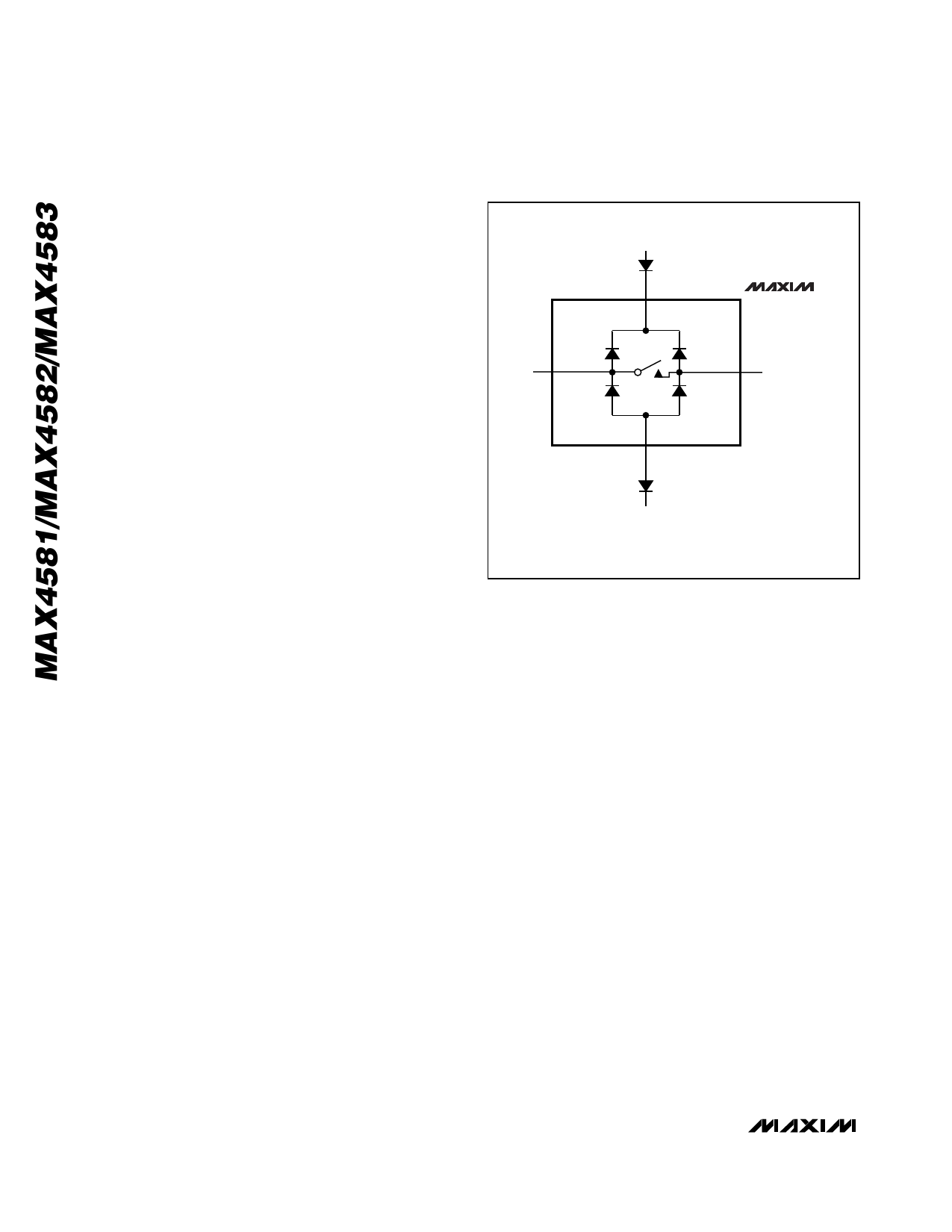
sequencing is not possible, add two small signal diodes
(D1, D2) in series with the supply pins for overvoltage
protection (Figure 1).
Adding diodes reduces the analog-signal range to one
diode drop below VCC and one diode drop above VEE,
but does not affect the devices’ low switch resistance
and low leakage characteristics. Device operation is
unchanged, and the difference between VCC and VEE
should not exceed 13V. These protection diodes are
not recommended when using a single supply if signal
levels must extend to ground.
High-Frequency Performance
In 50Ω systems, signal response is reasonably flat up
to 50MHz (see Typical Operating Characteristics).
Above 20MHz, the on response has several minor
peaks which are highly layout dependent. The problem
is not turning the switch on, but turning it off. The off-
state switch acts like a capacitor and passes higher
frequencies with less attenuation. At 10MHz, off isola-
tion is about -50dB in 50Ω systems, becoming worse
(approximately 20dB per decade) as frequency in-
creases. Higher circuit impedances also degrade off
isolation. Adjacent channel attenuation is about 3dB
above that of a bare IC socket and is entirely due to
capacitive coupling.
*
X, Y, Z
*
VCC
D1
EXTERNAL
BLOCKING DIODE
VCC
*
X_, Y_, Z_
*
MAX4581
MAX4582
MAX4583
VEE
D2
EXTERNAL
BLOCKING DIODE
VEE
*INTERNAL PROTECTION DIODES
Figure 1. Overvoltage Protection Using External Blocking
Diodes
Pin Nomenclature
The MAX4581/MAX4582/MAX4583 are pin-compatible
with the industry-standard 74HC4051/74HC4052/
74HC4053 and the MAX4051/MAX4052/MAX4053.
They function identically and have identical logic dia-
grams, although these parts differ electrically.
The pin designations and logic diagrams in this data
sheet conform to the original 1972 specifications pub-
lished by RCA for the CD4051/CD4052/CD4053. These
designations differ from the standard Maxim switch and
mux designations as found all other Maxim data sheets
(including the MAX4051/MAX4052/MAX4053) and may
cause confusion. Designers who feel more comfortable
with Maxim’s standard designations are advised that
the pin designations and logic diagrams on the
MAX4051/MAX4052/MAX4053 data sheet may be freely
applied to the MAX4581/MAX4582/MAX4583.
10 ______________________________________________________________________________________
Share Link: 