CS61884 データシートの表示(PDF) - Cirrus Logic
部品番号
コンポーネント説明
一致するリスト
CS61884 Datasheet PDF : 72 Pages
| |||
3.2 Control
SYMBOL
MCLK
MODE
CS61884
LQFP FBGA TYPE
DESCRIPTION
10
E1
Master Clock Input
This pin is a free running reference clock that should be
either 1.544 MHz for T1/J1 or 2.048 MHz for E1 operation.
This timing reference is used as follows:
- Timing reference for the clock recovery and jitter attenua-
tion circuitry.
- RCLK reference during Loss of Signal (LOS) conditions
I
- Transmit clock reference during Transmit all Ones (TAOS)
condition
- Wait state timing for microprocessor interface
- When this pin is held “High”, the PLL clock recovery cir-
cuit is disabled. In this mode, the CS61884 receivers
function as simple data slicers.
- When this pin is held “Low”, the receiver paths are pow-
ered down and the output pins RCLK, RPOS, and RNEG
are High-Z.
11
E2
Mode Select
This pin is used to select whether the CS61884 operates in
Serial host, Parallel host or Hardware mode.
Host Mode - The CS61884 is controlled through either a
serial or a parallel microprocessor interface (Refer to HOST
MODE (See Section 13 on page 32).
Hardware Mode - The microprocessor interface is disabled
and the device control/status are provided through the pins
on the device.
I
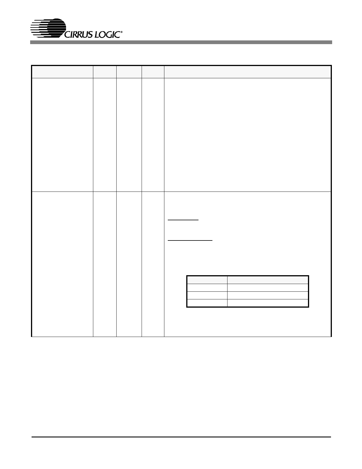
Table 1. Operation Mode Selection
Pin State
LOW
HIGH
VCCIO/2
OPERATING Mode
Hardware Mode
Parallel Host Mode
Serial Host Mode
NOTE: For serial host mode connect this pin to a resistor
divider consisting of two 10KΩ resistors between
VCCIO and GNDIO.
10
DS485PP4
Share Link: 