AMMCL002AWP-150I データシートの表示(PDF) - Advanced Micro Devices
部品番号
コンポーネント説明
一致するリスト
AMMCL002AWP-150I Datasheet PDF : 36 Pages
| |||
PRELIMINARY
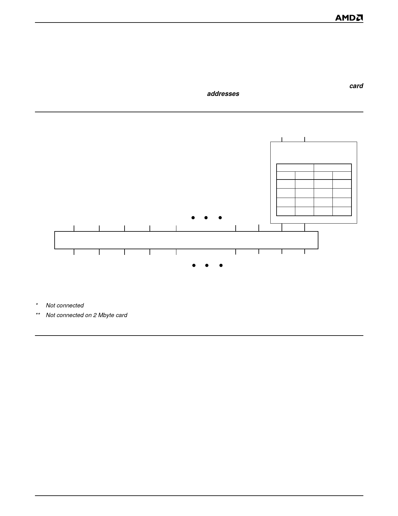
Data Accesses
The Miniature Card has a 16-bit data bus that can
accommodate word or byte accesses. By individually
asserting CEL# and CEH#, a host can access either
byte. However, byte swapping (moving the high byte
data to the low byte) is not supported.
Figure 2 shows the connections between the host and
Miniature Card. The host system address lines range
from A0–A25, whereas the Miniature Card address
lines range from A0–A24. On the host, A0 and the
byte/word line are sent to a decoder and output to
CEL# and CEH# on the Miniature Card. These two bits
enable a single device for byte accesses and two
devices for word accesses, as shown by the decoder
truth table in Figure 2. Again, the Miniature Card
address lines do not receive input from host address bit
A0. In this document, all address references are card
addresses, unless otherwise noted. Table 4 shows the
read/write modes for Miniature Cards.
Host Bus
A24
A25
A23 A22
A21
60-Pad Connector
A0 Byte/Word
A2
A1
Decoder
Decoder Truth Table
Input
Output
A0 B/W CEL# CEH#
0
0
0
0
0
1
0
1
1
0
0
0
1
1
1
0
A24* A23* A22* A21* A20**
Card Bus
A1
A0 CEL# CEH#
* Not connected
** Not connected on 2 Mbyte card
Figure 2. Host/Card Address Connections
21138E-3
Word-Wide Operations
The AMD Miniature Card provide the flexibility to
operate on data in a byte-wide or word-wide format. In
word-wide operations, the low bytes are controlled with
CEL#. The high bytes are controlled with CEH#. Refer to
the block diagram for more information.
Byte-Wide Operations
Byte-wide data is available for read and write opera-
tions (CEL# = 0, CEH# = 1). Even and odd bytes are
stored in separate memory devices (for example, S0
and S1) and are accessed by controlling CEL# and
CEH#. The even byte is the low order byte and the odd
byte is the high order byte of a 16-bit word.
Each memory sector or device pair must be addressed
separately for erase operations. Refer to the block
diagram for more information.
Card Detection
Each CD# (output) pin should be detected by the host
system to determine if the memory card is adequately
seated in the socket. CD# and CINS# are internally tied
to ground. If both bits are not detected, the system
should indicate that the card must be re-inserted.
Data Protection
An optional mechanical write protect switch provides
user-initiated write protection. When this switch is acti-
vated, WE# is internally forced high. The Flash memory
command register is disabled from accepting any write
commands. This prevents the card from responding to
any commands (for example, an Autoselect com-
mand). See Figure 3.
AmMCL00XA
9
Share Link: 