82559ER データシートの表示(PDF) - Intel
部品番号
コンポーネント説明
一致するリスト
82559ER Datasheet PDF : 94 Pages
| |||
GD82559ER — Networking Silicon
3.4
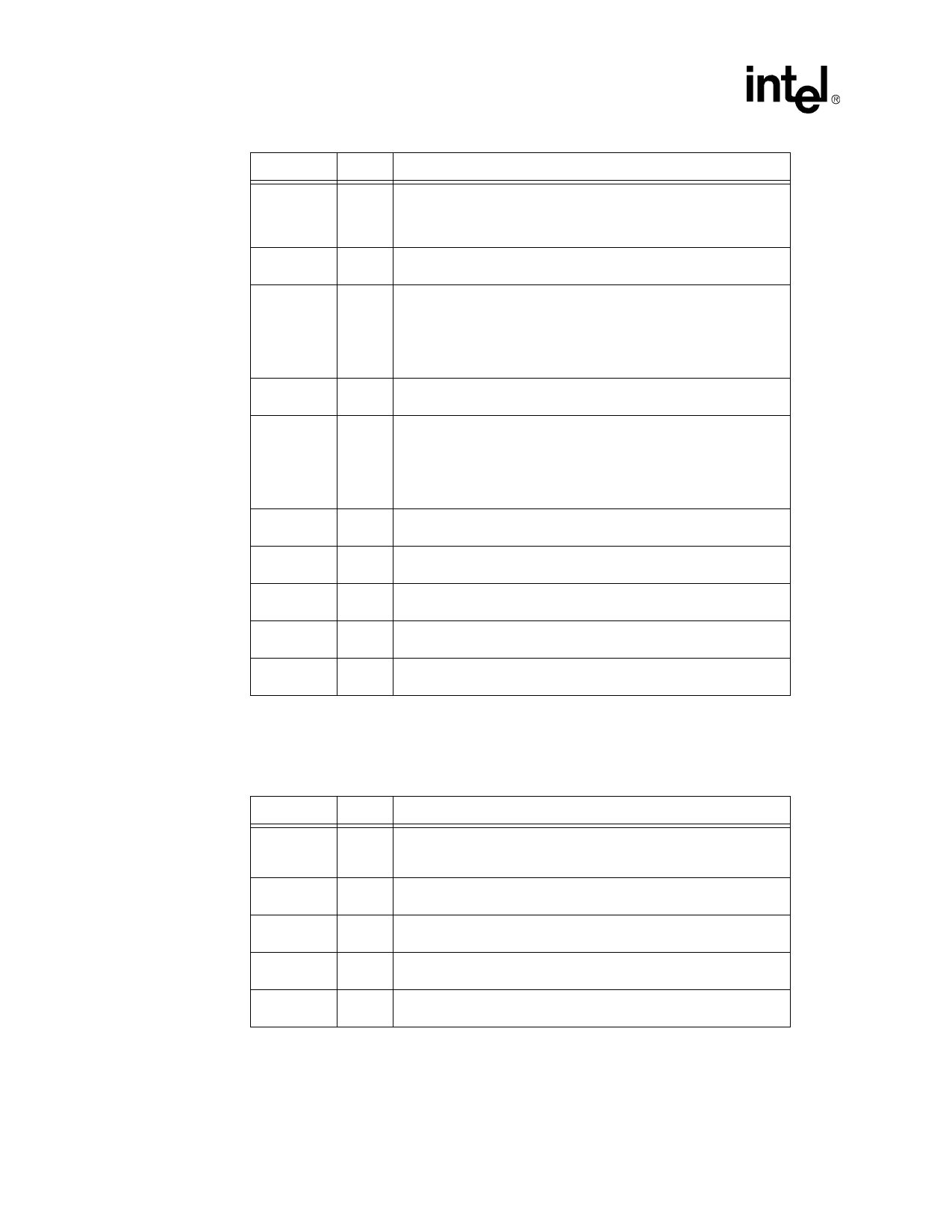
Symbol
FLA[13]/
EEDI
FLA[12:8]
FLA[7]/
CLKENB
FLA[6:2]
FLA[1]/
AUXPWR
FLA[0]
EECS
FLCS#
FLOE#
FLWE#
Type
OUT
OUT
T/S
OUT
T/S
T/S
OUT
OUT
OUT
OUT
Name and Function
Flash Address[13]/EEPROM Data Input. During Flash accesses,
this multiplexed pin acts as the Flash Address [13] output signal.
During EEPROM accesses, it acts as serial output data to the
EEPROM Data Input signal.
Flash Address[12:8]. These pins are used as Flash address outputs
to support 128 Kbyte Flash addressing.
Flash Address[7]/Clock Enable. This is a multiplexed pin and acts
as the Flash Address[7] output signal during nominal operation. When
the PCI RST# signal is active, this pin acts as input control over the
FLA[16]/CLK25 output signal. If the FLA[7]/CLKEN pin is connected to
a pull-up resistor (3.3 KΩ), a 25 MHz clock signal is provided on the
FLA[16]/CLK25 output; otherwise, it is used as FLA[16] output.
Flash Address[6:2]. These pins are used as Flash address outputs
to support 128 Kbyte Flash addressing.
Flash Address[1]/Auxiliary Power. This multiplexed pin acts as the
Flash Address[1] output signal during nominal operation. When RST is
active (low), it acts as the power supply indicator. If the 82559ER is fed
PCI power, this pin should be connected to a pull-down resistor; if the
82559ER is fed by auxiliary power, this pin should be connected to a
pull-up resistor.
Flash Address [0]. This pin acts as the Flash Address[0] output
signal during nominal operation.
EEPROM Chip Select. The EEPROM Chip Select signal is used to
assert chip select to the serial EEPROM.
Flash Chip Select. The Flash Chip Select signal is active during
Flash.
Flash Output Enable. This pin provides an active low output enable
control (read) to the Flash memory.
Flash Write Enable. This pin provides an active low write enable
control to the Flash memory.
Testability Port Signals
Symbol
TEST
TCK
TI
TEXEC
TO
Type
IN
IN
IN
IN
OUT
Name and Function
Test. If this input pin is high, the 82559ER will enable the test port.
During nominal operation this pin should be connected to a pull-down
resistor.
Testability Port Clock. This pin is used for the Testability Port Clock
signal.
Testability Port Data Input. This pin is used for the Testability Port
Data Input signal.
Testability Port Execute Enable. This pin is used for the Testability
Port Execute Enable signal.
Testability Port Data Output. This pin is used for the Testability Port
Data Output signal.
10
Datasheet
Share Link: 