82559ER データシートの表示(PDF) - Intel
部品番号
コンポーネント説明
一致するリスト
82559ER Datasheet PDF : 94 Pages
| |||
Networking Silicon — GD82559ER
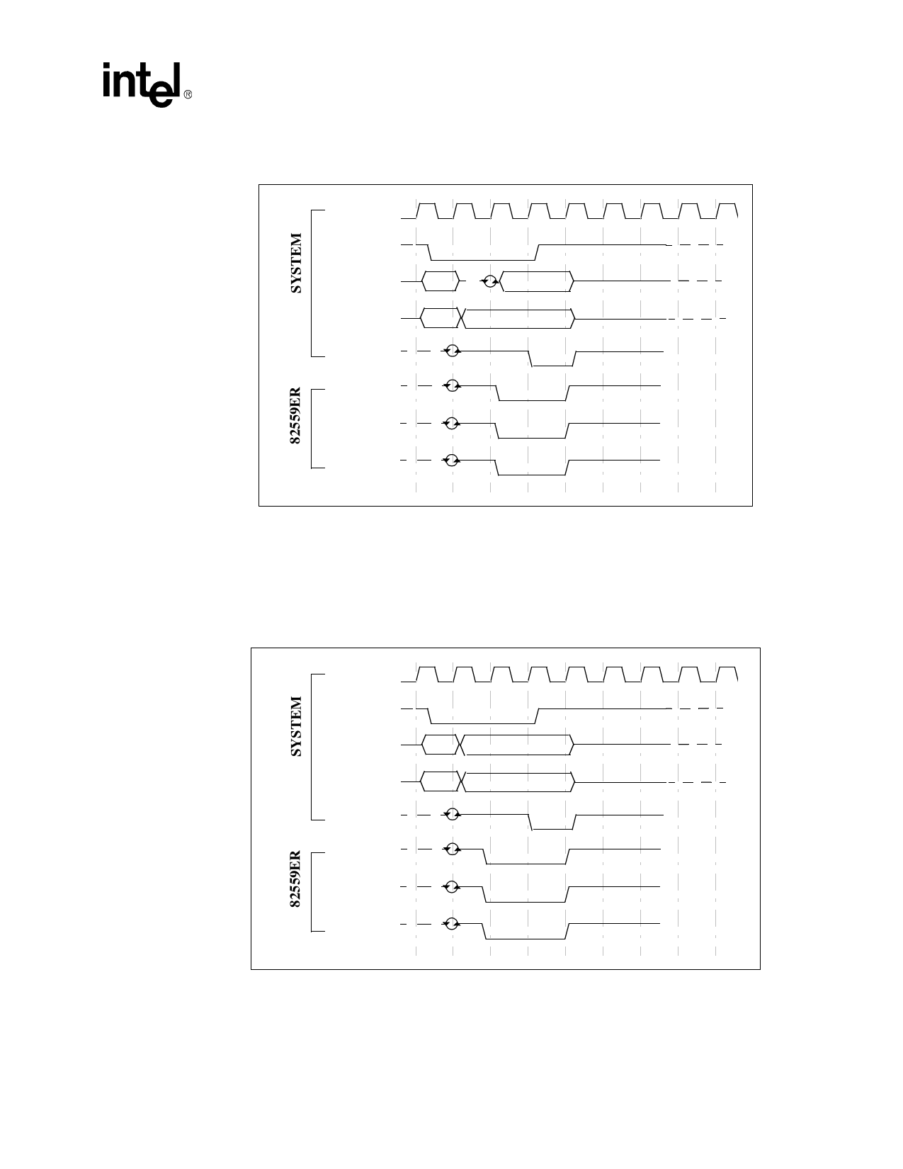
The figures below show CSR zero wait-state I/O read and write cycles. In the case of accessing the
Control/Status Registers, the CPU is the initiator and the 82559ER is the target of the transaction.
CLK
1
2
3
4
5
6
7
8
9
FRAME#
AD
ADDR
DATA
C/BE#
I/O RD
BE#
IRDY#
TRDY#
DEVSEL#
STOP#
Figure 2. CSR I/O Read Cycle
Read Accesses: The CPU, as the initiator, drives address lines AD[31:0], the command and byte
enable lines C/BE#[3:0] and the control lines IRDY# and FRAME#. As a slave, the 82559ER
controls the TRDY# signal and provides valid data on each data access. The 82559ER allows the
CPU to issue only one read cycle when it accesses the Control/Status Registers, generating a
disconnect by asserting the STOP# signal. The CPU can insert wait states by de-asserting IRDY#
when it is not ready.
CLK
1
2
3
4
5
6
7
8
9
FRAME#
AD
ADDR
DATA
C/BE#
I/O WR
BE#
IRDY#
TRDY#
DEVSEL#
STOP#
Figure 3. CSR I/O Write Cycle
Write Accesses: The CPU, as the initiator, drives the address lines AD[31:0], the command and
byte enable lines C/BE#[3:0] and the control lines IRDY# and FRAME#. It also provides the
82559ER with valid data on each data access immediately after asserting IRDY#. The 82559ER
Datasheet
15
Share Link: 