MC33166D2T データシートの表示(PDF) - Motorola => Freescale
部品番号
コンポーネント説明
一致するリスト
MC33166D2T Datasheet PDF : 16 Pages
| |||
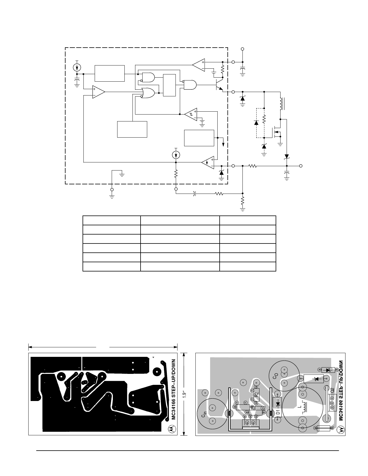
MC34166 MC33166
Figure 20. Step–Up/Down Converter
Vin
12 V
+
Oscillator
PWM
Thermal
ILIMIT
S
Q
R
UVLO
Reference
+
EA
4
+ Cin
330
Q1
2
D1
1N5822
D4
1N4148
+
1
D3
1N967A
R2
6.8 k
L
190 µH
*RG
620
Q2
MTP3055EL
D2
1N5822
CO +
1000
VO
28 V/0.6 A
3
5
CF
RF
0.47
4.7 k
R1
1.5 k
*Gate resistor RG, zener diode D3, and diode D4 are required only when Vin is greater than 20 V.
Test
Conditions
Results
Line Regulation
Load Regulation
Output Ripple
Short Circuit Current
Efficiency
Vin = 8.0 V to 24 V, IO = 0.6 A
Vin = 12 V, IO = 0.1 A to 0.6 A
Vin = 12 V, IO = 0.6 A
Vin = 12 V, RL = 0.1 Ω
Vin = 12 V, IO = 0.6 A
23 mV = ± 0.41%
3.0 mV = ± 0.005%
100 mVpp
4.0 A
82.8%
L = Coilcraft M1496–A or General Magnetics Technology GMT–0223, 42 turns of #16 AWG on
Magnetics Inc. 58350–A2 core.
Heatsink = AAVID Engineering Inc.
MC34166: 5903B, or 5930B
MTP3055EL: 5925B
Figure 20 shows that the MC34166 can be configured as a step–up/down converter with the addition of an external power MOSFET. Energy is stored in the
inductor during the on–time of transistors Q1 and Q2. During the off–time, the energy is transferred, with respect to ground, to the output filter capacitor and load.
This circuit configuration has two significant advantages over the basic step–up converter circuit. The first advantage is that output short–circuit protection is
provided by the MC34166, since Q1 is directly in series with Vin and the load. Second, the output voltage can be programmed to be less than Vin. Notice that during
the off–time, the inductor forward biases diodes D1 and D2, transferring its energy with respect to ground rather than with respect to Vin. When operating with Vin
greater than 20 V, a gate protection network is required for the MOSFET. The network consists of components RG, D3, and D4.
Figure 21. Step–Up/Down Converter Printed Circuit Board and Component Layout
3.45″
(Bottom View)
MOTOROLA ANALOG IC DEVICE DATA
+
Vin
+
–
ÎÎÎÎÎÎÎÎÎÎÎÎÎÎÎÎÎÎR–FVÎÎÎÎÎÎOR+1ÎÎÎÎÎÎCF ÎÎÎÎÎÎ
+
(Top View)
D3
D2 RGÎÎÎÎÎ
9
Share Link: 