MC33166D2T データシートの表示(PDF) - Motorola => Freescale
部品番号
コンポーネント説明
一致するリスト
MC33166D2T Datasheet PDF : 16 Pages
| |||
MC34166 MC33166
+
Oscillator
PWM
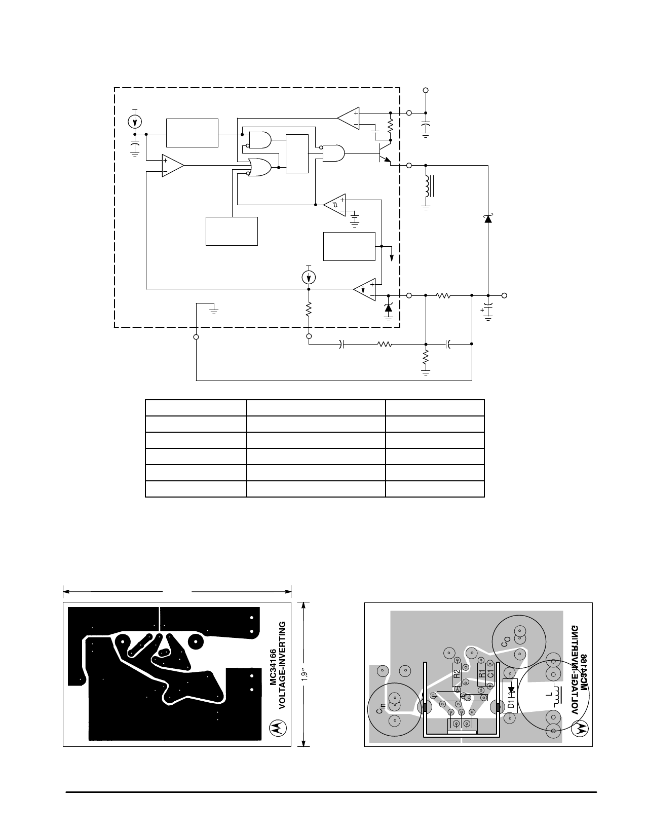
Figure 22. Voltage–Inverting Converter
Vin
12 V
ILIMIT
S
Q
R
UVLO
4
+ Cin
330
Q1
2
L
190 µH
Thermal
3
D1
1N5822
Reference
+
+
EA
R1
1
2.4 k
5
CF
RF
C1
0.47
4.7 k R2
0.047
3.3 k
VO
–12 V/1.0 A
CO
2200
Test
Conditions
Results
Line Regulation
Load Regulation
Output Ripple
Short Circuit Current
Efficiency
Vin = 8.0 V to 24 V, IO = 1.0 A
Vin = 12 V, IO = 0.1 A to 1.0 A
Vin = 12 V, IO = 1.0 A
Vin = 12 V, RL = 0.1 Ω
Vin = 12 V, IO = 1.0 A
3.0 mV = ± 0.01%
4.0 mV = ± 0.017%
80 mVpp
3.74 A
81.2%
L = Coilcraft M1496–A or General Magnetics Technology GMT–0223, 42 turns of #16 AWG on
Magnetics Inc. 58350–A2 core. Heatsink = AAVID Engineering Inc. 5903B, or 5930B.
Two potential problems arise when designing the standard voltage–inverting converter with the MC34166. First, the Switch Output emitter is limited to –1.5 V with
respect to the ground pin and second, the Error Amplifier’s noninverting input is internally committed to the reference and is not pinned out. Both of these problems
are resolved by connecting the IC ground pin to the converter’s negative output as shown in Figure 22. This keeps the emitter of Q1 positive with respect to the
ground pin and has the effect of reversing the Error Amplifier inputs. Note that the voltage drop across R1 is equal to 5.05 V when the output is in regulation.
Figure 23. Voltage–Inverting Converter Printed Circuit Board and Component Layout
3.0″
(Bottom View)
+
+
+
+
+ Vin –
+
ÎÎÎÎÎÎÎÎÎÎÎÎR–FÎÎÎÎÎÎVO +ÎÎÎÎÎÎCFÎÎÎÎÎÎ
+
(Top View)
10
MOTOROLA ANALOG IC DEVICE DATA
Share Link: 