MAAPGM0030-DIE データシートの表示(PDF) - Tyco Electronics
部品番号
コンポーネント説明
一致するリスト
MAAPGM0030-DIE Datasheet PDF : 6 Pages
| |||
5.0-9.0 GHz 1W Power Amplifier
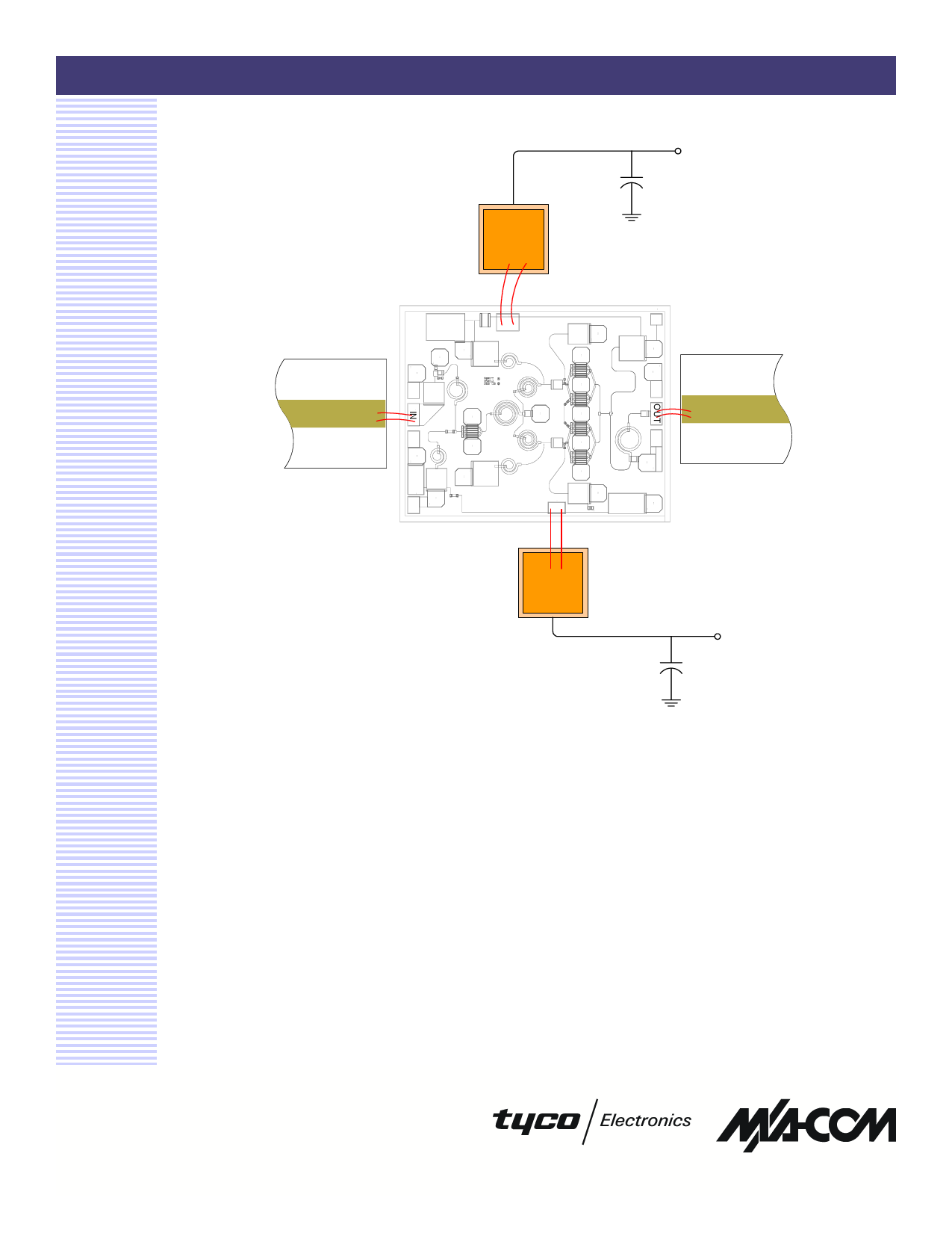
RFIN
100 pF
0.1 µF
RO-P-DS-3021 A 6/6
MAAPGM0030-DIE
VDD
VDD
RFOUT
VGG
100 pF
0.1 µF
VGG
Figure 6. Recommended bonding diagram for pedestal mount.
Support circuitry typical of MMIC characterization fixture for CW testing.
Assembly Instructions:
Die attach: Use AuSn (80/20) 1-2 mil. preform solder. Limit time @ 300 °C to less than 5 minutes.
Wirebonding: Bond @ 160 °C using standard ball or thermal compression wedge bond techniques. For
DC pad connections, use either ball or wedge bonds. For best RF performance, use wedge bonds of
shortest length, although ball bonds are also acceptable.
Biasing Note: Must apply negative bias to VGG before applying positive bias to VDD to prevent
damage to amplifier.
Specifications subject to change without notice.
Email: macom_adbu_ics@tycoelectronics.com
North America: Tel. (800) 366-2266
Asia/Pacific: Tel.+81-44-844-8296, Fax +81-44-844-8298
Europe: Tel. +44 (1908) 574 200, Fax+44 (1908) 574 300
Visit www.macom.com for additional data sheets and product information.
Share Link: 