QL5632 データシート - QuickLogic Corporation
Architecture Overview
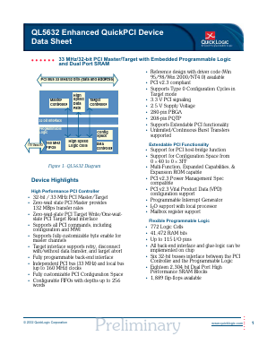
The QL5632 device in the QuickLogic® QuickPCI ESP (Embedded Standard Product) family provides a complete and customizable PCI interface solution combined with programmable logic. This device eliminates any need for the designer to worry about PCI bus compliance, yet allows for the maximum 32-bit PCI bus bandwidth (132 MBps).
Device Highlights
High Performance PCI Controller
• 32-bit / 33 MHz PCI Master/Target
• Zero-wait state PCI Master provides 132 MBps transfer rates
• Zero-wait-state PCI Target Write/One-waitstate PCI Target Read interface
• Supports all PCI commands, including configuration and MWI
• Supports fully-customizable byte enable for master channels
• Target interface supports retry, disconnect with/without data transfer, and target abort
• Fully programmable back-end interface
• Independent PCI bus (33 MHz) and local bus (up to 160 MHz) clocks
• Fully customizable PCI Configuration Space
• Configurable FIFOs with depths up to 256 words
• Reference design with driver code (Win 95/98/Win 2000/NT4.0) available
• PCI v2.3 compliant
• Supports Type 0 Configuration Cycles in Target mode
• 3.3 V PCI signaling
• 2.5 V Supply Voltage
• 280-pin PBGA
• 208-pin PQTP
• Supports Extendable PCI functionality
• Unlimited/Continuous Burst Transfers supported
Extendable PCI Functionality
• Support for PCI host-bridge function
• Support for Configuration Space from 0 × 40 to 0 × 3FF
• Multi-Function, Expanded Capabilities, & Expansion ROM capable
• PCI v2.3 Power Management Spec compatible
• PCI v2.3 Vital Product Data (VPD) configuration support
• Programmable Interrupt Generator
• I2O support with local processor
• Mailbox register support
Flexible Programmable Logic
• 772 Logic Cells
• 41,472 RAM bits
• Up to 115 I/O pins
• All back-end interface and glue-logic can be implemented on chip
• Six 32-bit busses interface between the PCI Controller and the Programmable Logic
• Eighteen 2,304 bit Dual Port High Performance SRAM Blocks
• 1,889 flip-flops available
