STW7NC90Z データシートの表示(PDF) - STMicroelectronics
部品番号
コンポーネント説明
一致するリスト
STW7NC90Z Datasheet PDF : 8 Pages
| |||
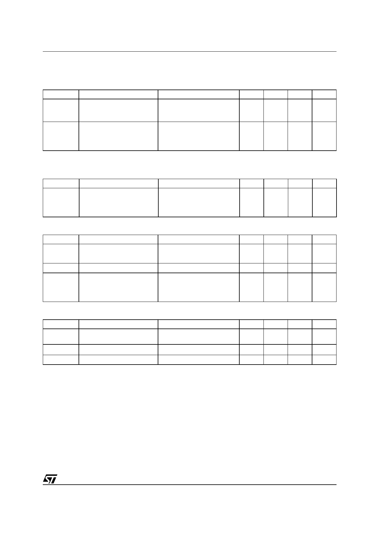
ELECTRICAL CHARACTERISTICS (CONTINUED)
SWITCHING ON (RESISTIVE LOAD)
Symbol
Parameter
td(on)
Turn-on Delay Time
tr
Rise Time
Qg
Total Gate Charge
Qgs
Gate-Source Charge
Qgd
Gate-Drain Charge
Test Conditions
VDD = 450V, ID = 3A
RG = 4.7Ω VGS = 10V
(see test circuit, Figure 3)
VDD = 720V, ID = 6 A,
VGS = 10V
STW7NC90Z
Min. Typ. Max. Unit
30
ns
12
ns
42
58.8
nC
13
nC
15
nC
SWITCHING OFF (INDUCTIVE LOAD)
Symbol
Parameter
tr(Voff)
Off-voltage Rise Time
tf
Fall Time
tc
Cross-over Time
Test Conditions
VDD = 720V, ID = 6 A,
RG = 4.7Ω, VGS = 10V
(see test circuit, Figure 5)
SOURCE DRAIN DIODE
Symbol
Parameter
Test Conditions
ISD
Source-drain Current
ISDM (2) Source-drain Current (pulsed)
VSD (1) Forward On Voltage
ISD = 6 A, VGS = 0
trr
Qrr
IRRM
Reverse Recovery Time
Reverse Recovery Charge
Reverse Recovery Current
ISD = 6 A, di/dt = 100A/µs,
VDD = 40 V, Tj = 150°C
(see test circuit, Figure 5)
GATE-SOURCE ZENER DIODE
Symbol
Parameter
Test Conditions
BVGSO
Gate-Source Breakdown
Voltage
Igs=± 1mA (Open Drain)
αT
Voltage Thermal Coefficient T=25°C Note(3)
Rz
Dynamic Resistance
IGS = 50 mA
Note: 1. Pulsed: Pulse duration = 300 µs, duty cycle 1.5 %.
2. Pulse width limited by safe operating area.
3. ∆VBV = αT (25°-T) BVGSO(25°)
Min.
Typ.
10
11
14
Max.
Unit
ns
ns
ns
Min. Typ. Max. Unit
6
A
24
A
1.6
V
680
ns
7.14
µC
21
A
Min.
25
Typ.
1.3
90
Max. Unit
V
10-4/°C
Ω
PROTECTION FEATURES OF GATE-TO-SOURCE ZENER DIODES
The built-in back-to-back Zener diodes have specifically been designed to enhance not only the device’s
ESD capability, but also to make them safely absorb possible voltage transients that may occasionally be
applied from gate to souce. In this respect the 25V Zener voltage is appropiate to achieve an efficient and
cost-effective intervention to protect the device’s integrity. These integrated Zener diodes thus avoid the
usage of external components.
3/8
Share Link: 