L9904(2002) データシートの表示(PDF) - STMicroelectronics
部品番号
コンポーネント説明
一致するリスト
L9904 Datasheet PDF : 17 Pages
| |||
L9904
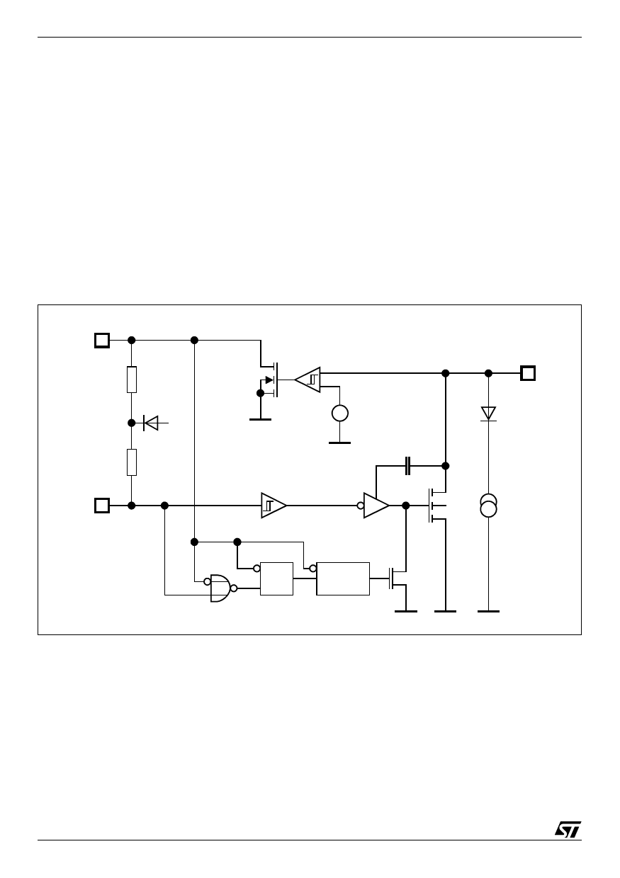
FUNCTIONAL DESCRIPTION (continued)
Undervoltage Shutdown
For supply voltages below the undervoltage disable threshold the gate driver remains in sink condition (L) and
the diagnostic DG is low.
Short Circuit Detection
The output voltage at the S1 and S2 pin of the H-Bridge is monitored by comparators to detect shorts to ground
or battery. The activated external highside MOS transistor will be switched off if the voltage drop remains below
the comparator threshold voltage VS1TH and VS2TH for longer than the short current detection time tSCd. The
transistor remains in off condition, the diagnostic output goes LOW until the DIR or PWM input status will be
changed. The status doesn't change for the other MOS transistors. The external lowside MOS transistor will be
switched off if the voltage drop passes over the comparator threshold voltage VS1TH and VS2TH for longer than
the short current detection time tSCd. The transistor remains in off condition, the diagnostic output goes LOW
until the DIR or PWM input status will be changed. The status doesn't change for the other MOS transistors.
Diagnostic Output (DG)
The diagnostic output provides a real time error detection, if monitors the following error stacks: Thermal shut-
down, overvoltage shutdown , undervoltage shutdown and short circuit shutdown. The open drain output with
internal pull up resistor is LOW if an error is occuring.
Bootstrap capacitor (CB1,CB2)
To ensure, that the external power MOS transistors reach the required RDSON, a minimum gate source voltage
of 5V for logic level and 10V for standard power MOS transistors has to be guaranteed. The highside transistors
require a gate voltage higher than the supply voltage. This is achieved with the internal chargepump circuit in
combination with the bootstrap capacitor. The bootstrap capacitor is charged, when the highside MOS transistor
is OFF and the lowside is ON. When the lowside is switched OFF, the charged bootstrap capacitor is able to
supply the gate driver of the highside power MOS transistor. For effective charging the values of the bootstrap
capacitors should be larger than the gate-source capacitance of the power MOS and respect the required PWM
ratio.
Chargepump circuit (CP)
The reverse battery protection can be obtained with an external N-channel MOS transistor as shown in fig.6. In
this case its drain-bulk diode provides the protection. The output CP is intended to drive the gate of this tran-
sistor above the battery voltage to switch on the MOS and to bypass the drain-bulk diode with the RDSON. The
CP has a connection to VS through an internal diode and a 20kΩ resistor.
Gate drivers for the external N-channel power MOS transistors (GH1, GH2, GL1, GL2)
High level at EN activates the driver of the external MOS under control of the DIR and PWM inputs (see truth
table and driving sequence fig.4). The external power MOS gates are connected via series resistors to the de-
vice to reduce electro magnetic emission (EME) of the system. The resistors influence the switching behaviour.
They have to be choosen carefully. Too large resistors enlarge the charging and discharging time of the power
MOS gate and can generate cross current in the halfbridges. The driver assures a longer switching delay time
from source to sink stage in order to prevent the cross conduction.
The gate source voltage is limited to 14V. The charge/discharge current is limited by the RDSON of the driver.
The drivers are not protected against shorts.
14/17
Share Link: 