ABA-53563-BLKG データシートの表示(PDF) - Broadcom Corporation
部品番号
コンポーネント説明
一致するリスト
ABA-53563-BLKG Datasheet PDF : 8 Pages
| |||
ABA-53563 Absolute Maximum Ratings[1]
Symbol Parameter
Vcc
Device Voltage, RF output to ground (T = 25°C)
Pin
CW RF Input Power (Vcc = 5V)
Pdiss
Total Power Dissipation[3]
Tj
Junction Temperature
TSTG
Storage Temperature
Units
V
dBm
W
°C
°C
Absolute Max.
+7
+20
0.47
150
-65 to 150
Thermal Resistance[2] (Vcc = 5V)
θjc = 117°C/W
Notes:
1. Operation of this device in excess of any of
these limits may cause permanent damage.
2. Thermal resistance measured using 150°C
Liquid Crystal Measurement Technique.
3. Board (package belly) temperature, Tb, is
25°C. Derate 5 mW/°C for Tb > 94.8°C.
Electrical Specifications
Tc = +25°C, Zo = 50 Ω, Pin = -30 dBm, Vcc = 5V, Freq = 2 GHz, unless stated otherwise.
Symbol
Parameter and Test Condition
Units
Min.
Typ.
Max.
Std Dev.
Gp[1]
∆Gp
NF[1]
P1dB[1]
OIP3[1]
VSWRin[1]
VSWRout[1]
Icc[1]
td[1]
Power Gain (|S21|2)
Power Gain Flatness,
f = 0.1 ~ 2.5 GHz
f = 0.1 ~ 3.5 GHz
Noise Figure
Output Power at 1dB Gain Compression
Output Third Order Intercept Point
Input VSWR
Output VSWR
Device Current
Group Delay
dB
20
21.5
0.2
dB
0.6
2.7
dB
3.5
4
0.11
dBm
12.7
0.14
dBm
22.9
0.14
1.1
1.2
mA
46
57
0.6
ps
160
Notes:
1. Measurements taken on 50Ω test board shown on Figure 1. Excess circuit losses had been de-embedded from actual measurements. Standard
deviation and typical data based on at least 500 parts sample size from 6 wafer lots. Future wafers allocated to this product may have nominal values
anywhere within the upper and lower spec limits.
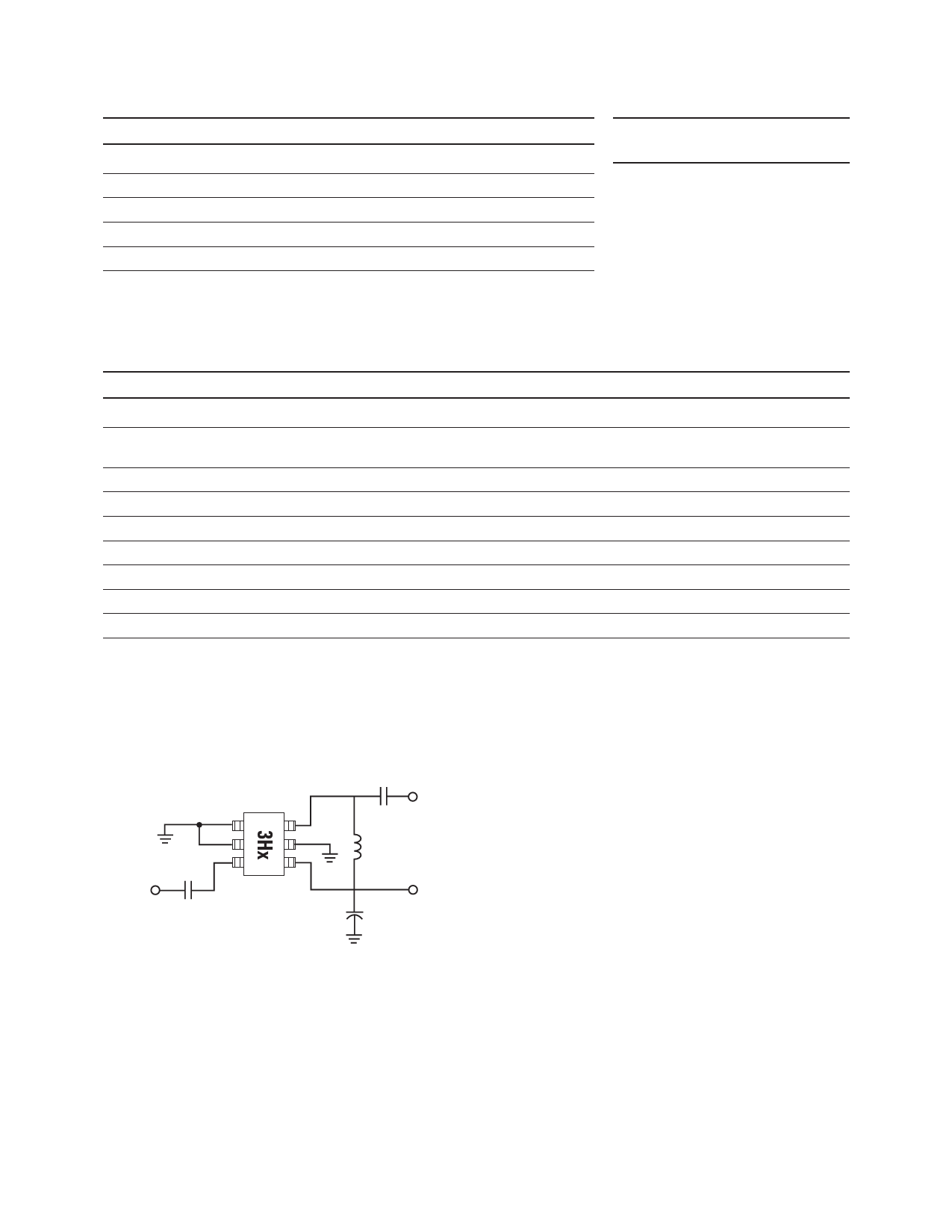
Cblock
RF Output
RF Input
Cblock
RFC
Vcc
Cbypass
Figure 1. ABA-53563 Production Test Circuit.
2
Share Link: 