HSP45116VC-25 データシートの表示(PDF) - Intersil
部品番号
コンポーネント説明
一致するリスト
HSP45116VC-25 Datasheet PDF : 18 Pages
| |||
HSP45116
Applications
The NCOM can be used for Amplitude, Phase and Frequency
modulation, as well as in variations and combinations of these
techniques, such as QAM. It is most effective in applications
requiring multiplication of a rotating complex sinusoid by an
external vector. These include AM and QAM modulators and
digital receivers. The NCOM implements AM and QAM
modulation on a single chip, and is a element in demodulation,
where it performs complex down conversion. It can be
combined with the Intersil HSP43220 Decimating Digital Filter
to form the front end of a digital receiver.
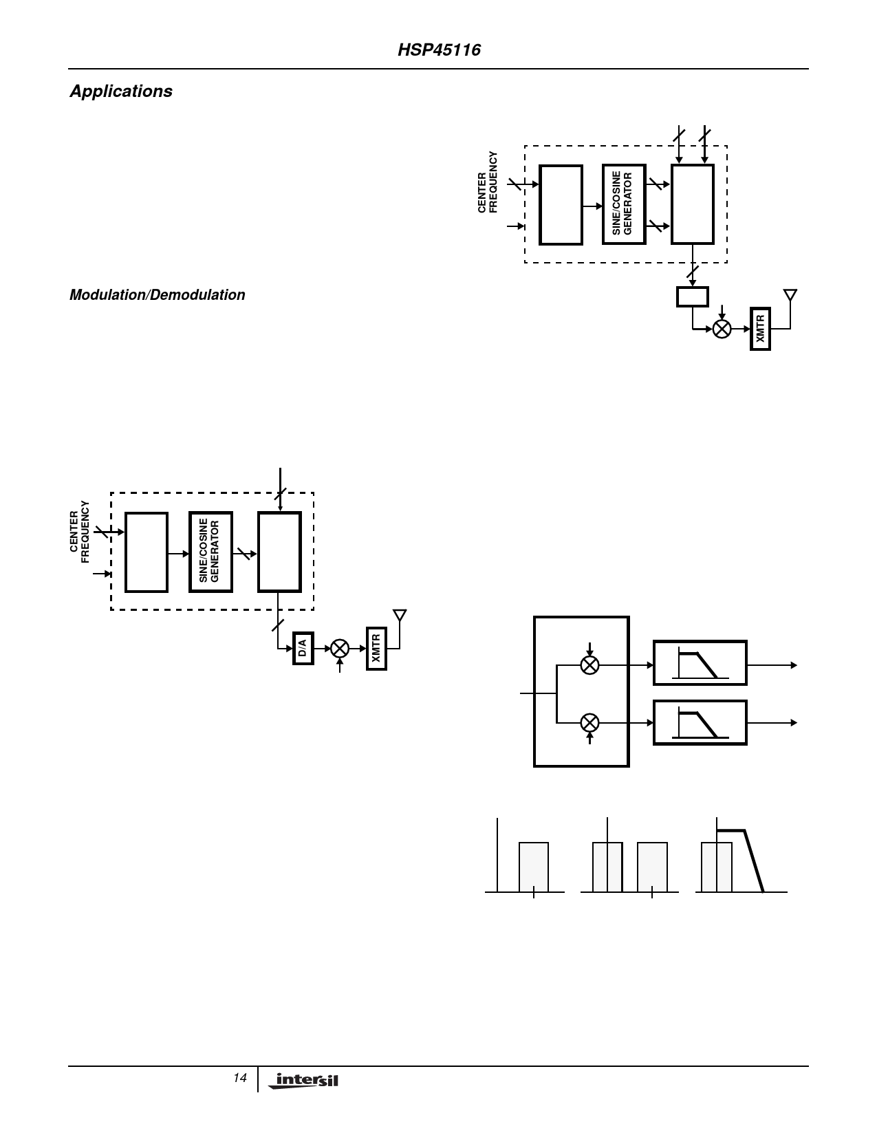
Modulation/Demodulation
Figure 4 shows a block diagram of an AM modulator. In this
example, the phase increment for the carrier frequency is
loaded into the center frequency register, and the
modulating input is clocked into the real input of the CMAC,
with the imaginary input set to 0. The modulated output is
obtained at the real output of the CMAC. With a sixteen bit,
two’s complement signal input, the output will be a 16-bit real
number, on ROUT0-15 (with OUTMUX = 00).
SIGNAL INPUT
16 RIN
32
CLK
PFCS
SIN
CMAC
16
NCOM
16 RO
MODULATED OUTPUT
32
CLK
PFCS
RIN IMIN
16
16
NCOM
16
CMAC
16
16 RO
D/A LO
FIGURE 5. QUADRATURE AMPLITUDE MODULATION (QAM)
The NCOM also works with the HSP43220 Decimating
Digital Filter to implement down conversion and low pass
filtering in a digital receiver (Figure 6). The NCOM performs
complex down conversion on the wideband input signal by
multiplying the input vector and the internally generated
complex sinusoid. The resulting signal has components at
twice the center frequency and at DC. Two HSP43220s, one
each on the real and imaginary outputs of the HSP45116,
perform low pass filtering and decimation on the down
converted data, resulting in a complex baseband signal.
HSP45116
NCOM
COS (wt)
HSP43220
DDF
LO
FIGURE 4. AMPLITUDE MODULATION
By replacing the real input with a complex vector, a similar
setup can generate QAM signals (Figure 5). In this case, the
carrier frequency is loaded into the center frequency register as
before, but the modulating vector now carries both amplitude
and phase information. Since the input vector and the internally
generated sine and cosine waves are both 16 bits, the number
of states is only limited by the characteristics of the
transmission medium and by the analog electronics in the
transmitter and receiver.
The phase and amplitude resolution for the Sine/Cosine section
(16-bit output), delivers a spectral purity of greater than 90dBc.
This means that the unwanted spectral components due to
phase uncertainty (phase noise) will be greater than 90dB
below the desired output (dBc, decibels below the carrier). With
a 32-bit phase accumulator in the Phase/Frequency Control
Section, the frequency tuning resolution equals the clock
frequency divided by 232. For example, a 25MHz clock gives a
tuning resolution of 0.006Hz.
SAMPLED
INPUT
DATA
SIN (wt)
INPUT
NCOM
OUTPUT
DDF
OUTPUT
0 10MHz
0 20MHz
0
FIGURE 6. CHANNELIZED RECEIVER CHIP SET
14
Share Link: 