HSP45116(1999) データシートの表示(PDF) - Intersil
部品番号
コンポーネント説明
一致するリスト
HSP45116 Datasheet PDF : 18 Pages
| |||
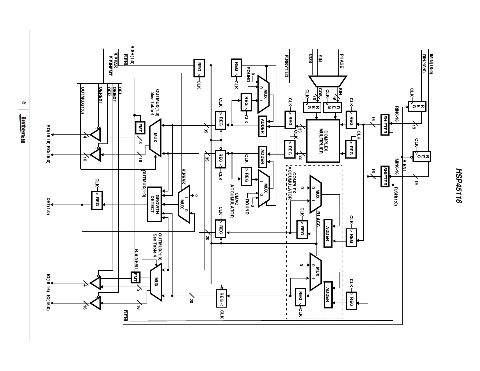
HSP45116
Pin Description (Continued)
NAME
NUMBER
TYPE
DESCRIPTION
PACO
L13
O Phase Accumulator Carry Output. Active low and registered by CLK. A low on this output
indicates that the phase accumulator has overflowed, i.e., the end of one sine/cosine cycle has
been reached.
TICO
P1
O Time Interval Accumulator Carry Output. Active low, registered by CLK. This output goes low
when a carry is generated by the time interval accumulator. This function is provided to time out
control events such as synchronizing register clocking to data timing.
RIN0-18
C1, C2, D1, D2, E1-
I
Real Input Data Bus. This is the external real component into the complex multiplier. The bus is
3, F1-3, G2, G3,
clocked into the real input data register by CLK when ENI is asserted; two’s complement.
H2, H3, J1-3, K1,
K2
IMIN0-18
A2-7, B2-7, C3-8,
D3
I
Imaginary Input Data Bus. This is the external imaginary component into the complex multiplier.
The bus is clocked into the real input data register by CLK when ENI is asserted; two’s
complement.
SH0-1
K3, L1
I
Shift Control Inputs. These lines control the input shifters of the RIN and IIN inputs of the
complex multiplier. The shift controls are common to the shifters on both of the busses.
ACC
L2
I
Accumulate/Dump Control. This input controls the complex accumulators and their holding
registers. When high, the accumulators accumulate and the holding registers are disabled.
When low, the feedback in the accumulators is zeroed to cause the accumulators to load.
The holding registers are enabled to clock in the results of the accumulation. This input is
registered by CLK.
BINFMT
N2
I
This input is used to convert the two’s complement output to offset binary (unsigned) for
applications using D/A converters. When low, bits RO19 and IO19 are inverted from the internal
two’s complement representation. This input is registered by CLK.
PEAK
M2
I
This input enables the peak detect feature of the block floating point detector. When high, the
maximum bit growth in the output holding registers is encoded and output on the DET0-1 pins.
When the PEAK input is asserted, the block floating point detector output will track the maximum
growth in the holding registers, including the data in the holding registers at the time that PEAK
is activated.
OUTMUX0-1
N12, N13
I
These inputs select the data to be output on RO0-19 and IO0-19.
RO0-19
C15, D14, D15,
E14, E15, F13-15,
G13-15, H13, H14,
J13, J14, K13-15,
L15, M15
O Real Output Data Bus. These Three-state outputs are controlled by OER and OEREXT.
OUTMUX0-1 select the data output on the bus.
IO0-19
A10-13, B8-15, C9- O Imaginary Output Data Bus. These Three-state outputs are controlled by OEI and OEIEXT.
14, D13, E13
OUTMUX0-1 select the data output on the bus.
DET0-1
N15, L14
O These output pins indicate the number of bits of growth in the accumulators. While PEAK is low,
these pins indicate the peak growth. The detector examines bits 15-18, real and imaginary
accumulator holding registers and bits 30-33 of the real and imaginary CMAC holding registers.
The bits indicate the largest growth of the four registers.
OER
P14
I
Three-state control for bits RO0-15. Outputs are enabled when the line is low.
OEREXT
M13
I
Three-state control for bits RO16-19. Outputs are enabled when the line is low.
OEI
M14
I
Three-state control for bits IO0-15. Outputs are enabled when the line is low.
OEIEXT
N14
I
Three-state control for bits IO16-19. Outputs are enabled when the line is low.
6
Share Link: 