NCV8664C データシートの表示(PDF) - ON Semiconductor
部品番号
コンポーネント説明
一致するリスト
NCV8664C Datasheet PDF : 16 Pages
| |||
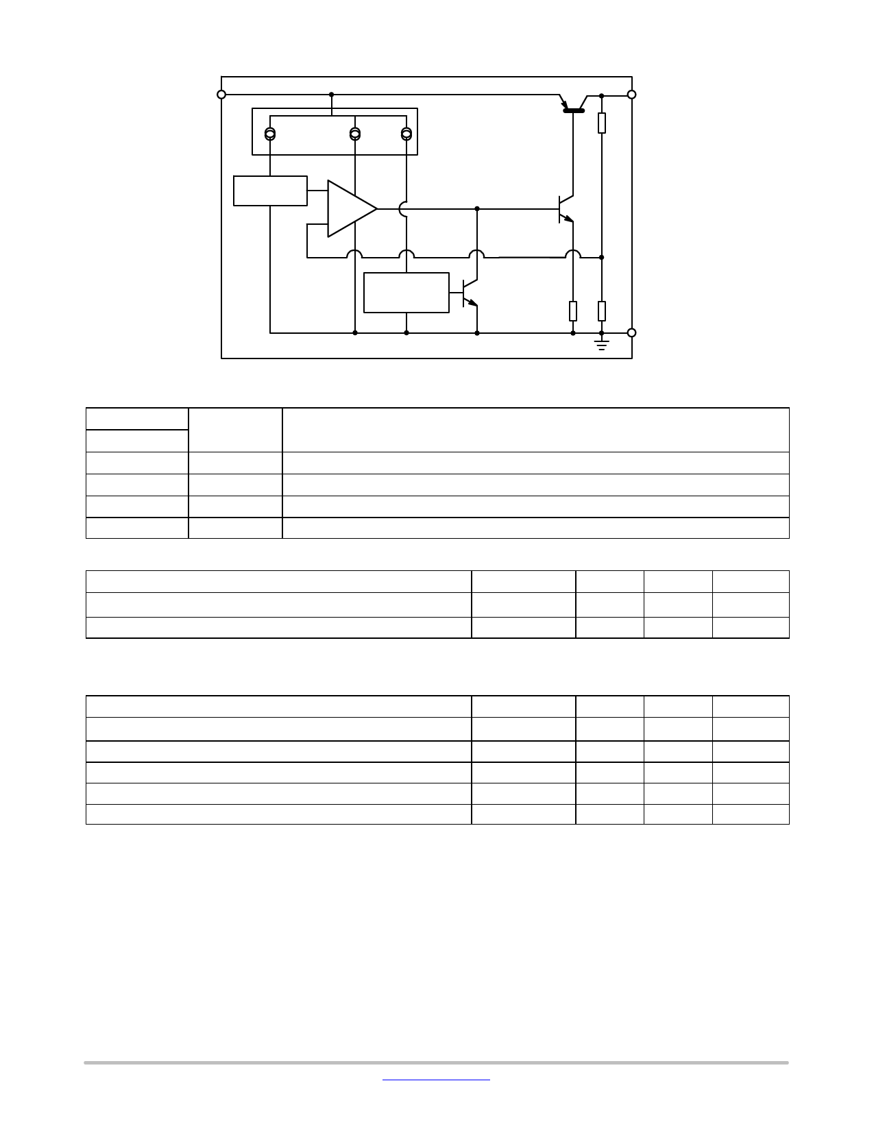
VIN
Bias Current
Generators
1.3 V
Reference
+
Error
Amp
-
NCV8664C
VOUT
Thermal
Shutdown
GND
PIN FUNCTION DESCRIPTION
Pin No.
DPAK/SOT−223
Symbol
1
VIN
2
GND
3
4, TAB
VOUT
GND
Figure 1. Block Diagram
Function
Unregulated input voltage; 4.5 V to 45 V.
Ground; Must be connected to GND potential.
Regulated output voltage.
Ground; substrate and best thermal connection to the die.
OPERATING RANGE
Pin Symbol, Parameter
Symbol
Min
Max
Unit
VIN, DC Input Operating Voltage
VIN
4.5
+45
V
Junction Temperature Operating Range
TJ
−40
+150
°C
Functional operation above the stresses listed in the Recommended Operating Ranges is not implied. Extended exposure to stresses beyond the
Recommended Operating Ranges limits may affect device reliability.
MAXIMUM RATINGS
Rating
Symbol
Min
Max
Unit
VIN, DC Voltage
VIN
−42
+45
V
VOUT, DC Voltage
VOUT
−0.3
+32
V
Storage Temperature
Tstg
−55
+150
°C
ESD Capability, Human Body Model (Note 1)
VESDHBM
4
−
kV
ESD Capability, Machine Model (Note 1)
VESDMIM
200
−
V
Stresses exceeding those listed in the Maximum Ratings table may damage the device. If any of these limits are exceeded, device functionality
should not be assumed, damage may occur and reliability may be affected.
1. This device series incorporates ESD protection and is tested by the following methods:
ESD HBM tested per AEC−Q100−002 (EIA/JESD22−A 114C)
ESD MM tested per AEC−Q100−003 (EIA/JESD22−A 115C)
www.onsemi.com
2
Share Link: 