SPX1129M3-3.3/TR データシートの表示(PDF) - Signal Processing Technologies
部品番号
コンポーネント説明
一致するリスト
SPX1129M3-3.3/TR Datasheet PDF : 8 Pages
| |||
Power Dissipation ........................................................ Internally Limited
Lead Temp. (Soldering, 5 Seconds) ............................................. 260°C
Storage Temperature Range ........................................ -65°C to +150°C
Operating Junction Temperature Range ....................... -40°C to +125°C
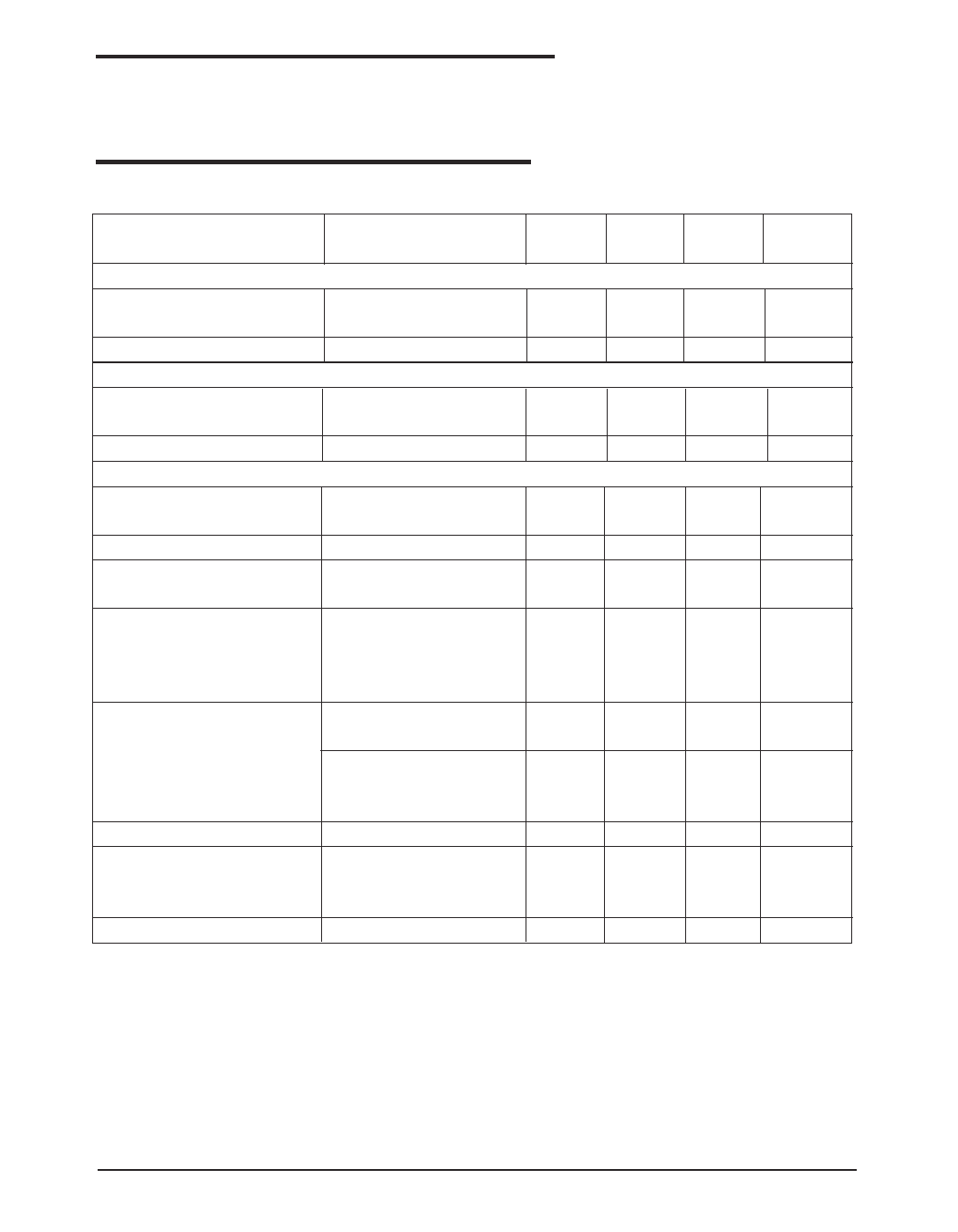
ABSOLUTE MAXIMUM RATINGS
Input Supply Voltage ....................................................... -20V to +20V
ESD Rating .............................................................................. 2kV Min
ELECTRICAL CHARACTERISTICS
Electrical characteristics at VIN = 6V, IO = 1mA, COUT = 2.2µF, TA= 25°C, unless otherwise specified. Boldface applies over
the full operating temperature range.
PARAMETER
CONDITIONS
(Note 2)
TYP
MIN
MAX
UNITS
3.3V Version
Output Voltage
Reverse Output Current
5.0V Version
1mA ≤ IL ≤ 400mA
VOUT= 3.3V, VIN= 0V
3.3
3.267 3.333
V
3.3
3.217 3.382
16
25
µA
Output Voltage
5.0
4.950 5.050
V
Reverse Output Current
All Voltage Options
1mA ≤ IL ≤ 400mA
VOUT= 5.0V, VIN= 0V
5.0
4.880 5.120
16
25
µA
Output Voltage
Temperature Coefficient
(Note1)
20
100
ppm/°C
Line Regulation
6V ≤ VIN ≤ 20V (Note 4)
1.5
Load Regulation (Note 3)
IL=1 to 400mA
6
10
mV
20
mV
30
Dropout Voltage (Note 5)
IL=1mA
0.13
0.17
V
0.25
IL=400mA
0.42
0.55
0.70
Ground Current
IL=1mA
100
IL=10mA
350
IL=50mA
1.5
IL=100mA
2
IL=400mA
7
Current Limit
VOUT=0
330
Ripple Rejection
VIN -VOUT=1V(Avg),
58
VRIPPLE=0.5Vp-p, FRIPPLE=120Hz,
ILOAD=400mA, TJ= 25°C
Input Reverse Leakage Current VIN= -20V, VOUT=0V
200
µA
500
3
mA
6
25
800
mA
50
dB
1.0
mA
Note 1: Output or reference voltage temperature coefficients defined as the worst case voltage change divided by
the total temperature range.
Note 2: Unless otherwise specified all limits are guaranteed for Tj = 25°C, VIN = 6V, IL = 1mA and CL = 2.2µF.
Note 3: Regulation is measured at constant junction temperature, using pulse testing with a low duty cycle. Changes
in output voltage due to heating effects are covered under the specification for thermal regulation.
Note 4: Line regulation for the SPX1129 is tested at 25°C for IL = 1 mA. For TJ = 125°C, line regulation is guaranteed
by design.
Note 5: Dropout voltage is defined as the input to output differential at which the output voltage drops 100 mV below
its nominal value measured at 1V differential.
Date: 5/25/04
SPX1129 400mA Low Dropout Voltage Regulator
2
©Copyright 2004 Sipex Corporation
Share Link: 